UA5M15MP
5 - 18GHz Surface Mount Amplifier
with Integrated Bias
Features
• Wide operating range: 5-18GHz
• 3.3V, 100mA drain bias (gate N/C)
for gain and NF:
▪ 13 ±0.4dB gain, 7dB NF, 16dBm
Psat, 13.5dBm P1dB
• 5V, 130mA drain bias (gate N/C)
for power:
▪ 12.5 ±0.7dB gain, 9dB NF,
19.5dBm Psat, 17dBm P1dB
• Single supply voltage with
self-biasing gate OR direct control
of both gate and drain stages
Description
The UA5M15MP is a two-stage pHEMT
amplifier MMIC in a Pb-free leadless plastic
QFN package. The IC features a positive
gain slope that offsets package loss, resulting
in a SMT part with excellent gain flatness
across a broad bandwidth. The device
can be operated at 5V 130mA for power
applications, or 3.3V 100mA for low-noise
and gain.
Surface Mount Package
•
•
16-pin Pb-free SMT QFN package
3x3mm pkg size; 0.5mm pad pitch
Application
The UA5M15MP is ideally suited for:
• Point-to-point and point-to-multipoint
digital radio
• Spread spectrum broadband communications
• LO driver or mixer isolation amplifier
• General isolation and gain block
amplifier
Functional Diagram
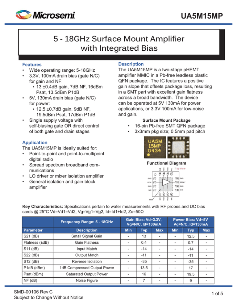
Key Characteristics: Specifications pertain to wafer measurements with RF probes and DC bias
cards @ 25°C Vd=Vd1=Vd2, Vg=Vg1=Vg2, Id=Id1+Id2, Zo=50Ω
Frequency Range: 5 - 18GHz
Parameter
Gain Bias: Vd=3.3V,
Vg=N/C, Id=100mA
Power Bias: Vd=5V
Vg=N/C, Id=130mA
Description
Min
Typ
Max
Min
Typ
Max
Small Signal Gain
-
13
-
-
12.5
-
Gain Flatness
-
0.4
-
-
0.7
-
S11 (dB)
Input Match
-
-14
-
-
-14
-
S22 (dB)
Output Match
-
-11
-
-
-11
-
S12 (dB)
Reverse Isolation
-
-35
-
-
-35
-
P1dB (dBm)
1dB Compressed Output Power
-
13.5
-
-
17
-
Psat (dBm)
Saturated Output Power
-
16
-
-
19.5
-
Noise Figure
-
7
-
-
9
-
S21 (dB)
Flatness (±dB)
NF (dB)
SMD-00106 Rev C
Subject to Change Without Notice
1 of 5
UA5M15MP
Typical Probed Performance QFN Package
S21
S11, S22
S12
Group Delay
SMD-00106 Rev C
Subject to Change Without Notice
2 of 5
UA5M15MP
Supplemental Tested in Evaluation Fixture
S21
Output Power
S11, S22
Noise Figure
S12
Group Delay
SMD-00106 Rev C
Subject to Change Without Notice
3 of 5
UA5M15MP
Table 1: Supplemental Specifications
Parameter
Description
Min
Typ
Max
Vd1
Drain Bias Voltage FET1
-
3.3V, 5V
6V
Id1
Drain Bias Current FET1
-
-
90mA
Vd2
Drain Bias Voltage FET1
-
3.3V, 5V
6V
Id2
Drain Bias Current FET1
-
-
110mA
Vgg1
Drain Bias Current FET1
-4
N/C
+1V
Vgg2
Drain Bias Current FET1
-4
N/C
+1V
Pin
Input Power (CW)
-
-
12dBm
Pdc
Power Dissipation
-
0.33W, 0.65W
-
Tch
Channel Temperature
-
-
150˚C
Θch
Thermal Resistance (Tcase=85˚C)
-
60˚C/W
Caution, ESD
Sensitive Device
-
TSTORAGE
Storage Temperature1
-65˚C
1 Passed temperature cyling per JESD22-A104C, -65°C to +150°C, 250 cycles, dwells of 1
minute, 10°C/minute minimum ramp rate.
150˚C
Functional Block Diagram
Table 2: Typical Bias Values
Vdd (V)
Idd (mA)
App
+5.0
130
Power
+4.0
110
-
+3.3
100
Gain
+2.5
79
Low-noise
Table 3: Pin Descriptions
Number
Function
Description
4, 5, 8, 9, 13, 16
N/C
No connection necessary, may be connected
to DC/RF ground
1, 3, 10, 12, + paddle
GND
Must be connected to DC/RF ground
2, 11
RF IN, OUT
AC coupled and matched to 50W
6, 7
VG1, VG2
Optional 1st and 2nd gate bias lines, required > 100pF
low-freq bypass capacitor if used
14, 15
VD1, VD2
1st and 2nd drain bias lines, requires>100pF low-freq
bypass capacitor and clean power supply
SMD-00106 Rev C
Subject to Change Without Notice
4 of 5
UA5M15MP
QB Package Outline
Package Notes:
• Conforms to JEDEC MO-220, revision 1
• Pin 1 ID indicated by dot on top of package
• All units millimeters, not to scale
• Pkg is 100% Pb free (lead free)
• Leadframe base is 0.2mm Cu 194 FH with
Ag-ring finish
• Solder plate is 100% Sn
• All ground leads and center paddle must
be connected to RF ground
Lead Free (Pb-free):
The UA5M15MP QFN package contains no lead (Pb) and eliminates the need for costly
re-qualification efforts, which are necessary to conform to the European mandated “Restricted
use of Hazardous Substances” (RoHS) compliance.
Thermal Heat Sinking:
To avoid damage and for optimum performance, you must observe the maximum channel
temperature and ensure adequate heat sinking. PCB ground planes are not sufficient, the backside
of the QFN must be soldered to the PCB, and PCB filled or plated vias must be used to conduct
heat away from this contact.
ESD Handling and Bonding:
This package is ESD sensitive; preventive measures should be taken during handling and solder
attach. Solder paste and flux screen printing is recommended.
SMD-00106 Rev C
Subject to Change Without Notice
5 of 5
UA5M15MP
Information contained in this document is proprietary to Microsem. This document may not be modified in any way without the express
written consent of Microsemi. Product processing does not necessarily include testing of all parameters. Microsemi reserves the right to
change the configuration and performance of the product and to discontinue product at any time.
Microsemi Corporate Headquarters
Microsemi Corporation (Nasdaq: MSCC) offers a comprehensive portfolio of semiconductor
One Enterprise, Aliso Viejo CA 92656 USA and system solutions for communications, defense and security, aerospace, and industrial
Within the USA: +1 (949) 380-6100
markets. Products include high-performance and radiation-hardened analog mixed-signal
Sales: +1 (949) 380-6136
integrated circuits, FPGAs, SoCs, and ASICs; power management products; timing and
Fax: +1 (949) 215-4996
synchronization devices and precise time solutions, setting the world’s standard for time;
voice processing devices; RF solutions; discrete components; security technologies and
scalable anti-tamper products; Power-over-Ethernet ICs and midspans; as well as custom
design capabilities and services. Microsemi is headquartered in Aliso Viejo, Calif. and has
approximately 3,400 employees globally. Learn more at www.microsemi.com.
© 2014 Microsemi Corporation. All rights reserved. Microsemi and the Microsemi logo are trademarks of Microsemi Corporation. All other
trademarks and service marks are the property of their respective owners.
SMD-00106 Rev C
Subject to Change Without Notice
6 of 5


