Preliminary Technical Data
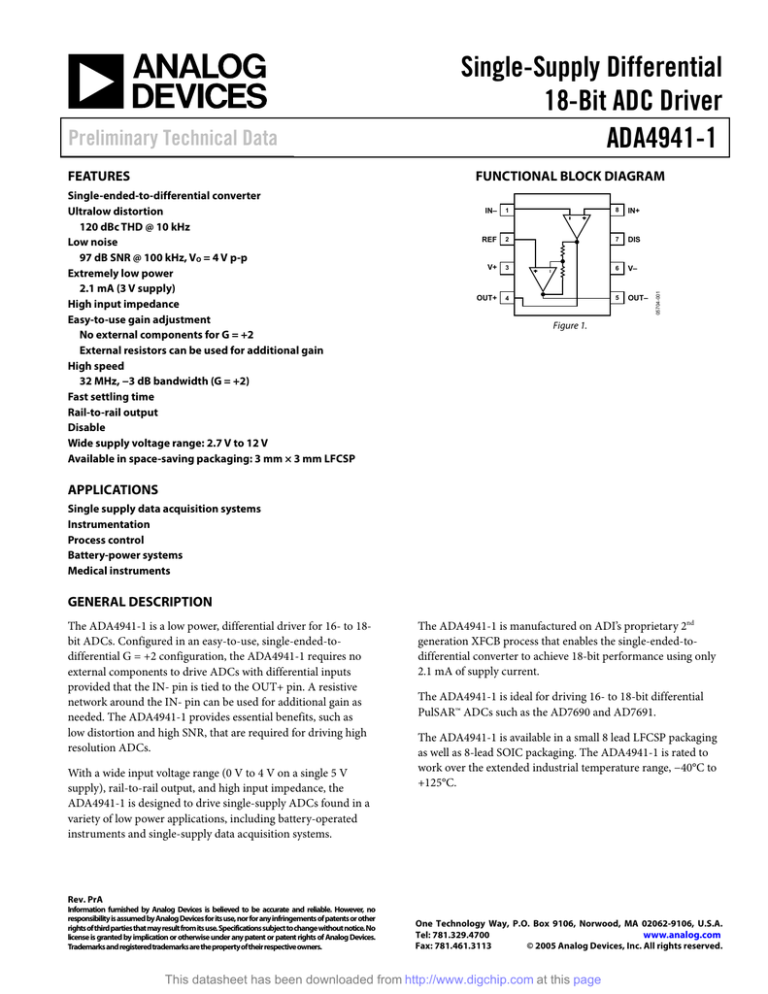
FUNCTIONAL BLOCK DIAGRAM
Single-ended-to-differential converter
Ultralow distortion
120 dBc THD @ 10 kHz
Low noise
97 dB SNR @ 100 kHz, VO = 4 V p-p
Extremely low power
2.1 mA (3 V supply)
High input impedance
Easy-to-use gain adjustment
No external components for G = +2
External resistors can be used for additional gain
High speed
32 MHz, −3 dB bandwidth (G = +2)
Fast settling time
Rail-to-rail output
Disable
Wide supply voltage range: 2.7 V to 12 V
Available in space-saving packaging: 3 mm × 3 mm LFCSP
IN–
1
8
IN+
REF
2
7
DIS
V+
3
6
V–
OUT+
4
5
OUT–
05704-001
FEATURES
Single-Supply Differential
18-Bit ADC Driver
ADA4941-1
Figure 1.
APPLICATIONS
Single supply data acquisition systems
Instrumentation
Process control
Battery-power systems
Medical instruments
GENERAL DESCRIPTION
The ADA4941-1 is a low power, differential driver for 16- to 18bit ADCs. Configured in an easy-to-use, single-ended-todifferential G = +2 configuration, the ADA4941-1 requires no
external components to drive ADCs with differential inputs
provided that the IN- pin is tied to the OUT+ pin. A resistive
network around the IN- pin can be used for additional gain as
needed. The ADA4941-1 provides essential benefits, such as
low distortion and high SNR, that are required for driving high
resolution ADCs.
With a wide input voltage range (0 V to 4 V on a single 5 V
supply), rail-to-rail output, and high input impedance, the
ADA4941-1 is designed to drive single-supply ADCs found in a
variety of low power applications, including battery-operated
instruments and single-supply data acquisition systems.
The ADA4941-1 is manufactured on ADI’s proprietary 2nd
generation XFCB process that enables the single-ended-todifferential converter to achieve 18-bit performance using only
2.1 mA of supply current.
The ADA4941-1 is ideal for driving 16- to 18-bit differential
PulSAR™ ADCs such as the AD7690 and AD7691.
The ADA4941-1 is available in a small 8 lead LFCSP packaging
as well as 8-lead SOIC packaging. The ADA4941-1 is rated to
work over the extended industrial temperature range, −40°C to
+125°C.
Rev. PrA
Information furnished by Analog Devices is believed to be accurate and reliable. However, no
responsibility is assumed by Analog Devices for its use, nor for any infringements of patents or other
rights of third parties that may result from its use. Specifications subject to change without notice. No
license is granted by implication or otherwise under any patent or patent rights of Analog Devices.
Trademarks and registered trademarks are the property of their respective owners.
One Technology Way, P.O. Box 9106, Norwood, MA 02062-9106, U.S.A.
Tel: 781.329.4700
www.analog.com
Fax: 781.461.3113
© 2005 Analog Devices, Inc. All rights reserved.
This datasheet has been downloaded from http://www.digchip.com at this page
ADA4941-1
Preliminary Technical Data
TABLE 0F CONTENTS
Features .............................................................................................. 1
Specifications .....................................................................................3
Applications....................................................................................... 1
Outline Dimensions ..........................................................................6
Functional Block Diagram .............................................................. 1
Ordering Guide .............................................................................6
General Description ......................................................................... 1
REVISION HISTORY
10/05—Revision PrA: Preliminary Version
Rev. PrA | Page 2 of 6
Preliminary Technical Data
ADA4941-1
SPECIFICATIONS
TA = 25°C, VS = 3 V, unless otherwise noted.
Table 1.
Parameter
DYNAMIC PERFORMANCE
−3 dB Bandwidth
Overdrive Recovery Time
Slew Rate
Settling Time 0.0004%
NOISE/DISTORTION PERFORMANCE
THD
SNR
RTO Voltage Noise
Input Current Noise
DC PERFORMANCE
Differential Input Offset Voltage
Differential Input Offset Voltage Drift
Common-Mode Offset Voltage
Common-Mode Offset Voltage Drift
Input Bias Current
Input Offset Current
Gain
Gain Error
Gain Error Drift
INPUT CHARACTERISTICS
Input Resistance
Input Capacitance
Input Common-Mode Voltage Range
Common-Mode Rejection Ratio
OUTPUT CHARACTERISTICS
Output Voltage Swing: VON
VOP
Output Current
Capacitive Load Drive
POWER SUPPLY
Operating Range
Quiescent Current
Quiescent Current—Disable
Power Supply Rejection Ration
+PSRR
−PSRR
DISABLE
VDIS High
VDIS Low
Input Current VDIS = HIGH/LOW
Turn-On Time
Turn-Off Time
Conditions
Min
VO = 0.1 V p-p
VO = 2.0 V p-p
VO = 2 V step
VO = 2 V p-p step
fC = 10 kHz, VO = 2 V p-p
fC = 1 MHz, VO = 2 V p-p
fC = 100 kHz, VO = 2 V p-p
f = 100 kHz
f = 100 kHz
Typ
Unit
30
6.6
300
22.5
0.3
MHz
MHz
ns
V/μs
μs
105
57
91
dBc
dBc
dB
nV/√Hz
pA/√Hz
1
0.2
IN and REF
IN and REF
(+OUT − −OUT)/(IN − REF)
2.2
0.2
2
0.1
0.01
IN and REF
IN and REF
12
2
0.1
.5
2
VCM =±2.5 V
110
RL = 1kΩ
RL = 1kΩ
0.1 to 2.9
0.1 to 2.9
25
2.7
Rev. PrA| Page 3 of 6
Max
mV
μV/°C
mV
μV/°C
μA
μA
V/V
%
%/°C
MΩ
pF
V
dB
V
V
mA
pF
2.1
30
12
V
mA
μA
110
110
dB
dB
1.8
1.6
5/10
30
0.65
V
V
μA
μs
μs
ADA4941-1
Preliminary Technical Data
TA = 25°C, VS = 5 V, unless otherwise noted.
Table 2.
Parameter
DYNAMIC PERFORMANCE
−3 dB Bandwidth
Overdrive Recovery Time
Slew Rate
Settling Time 0.0004%
NOISE/DISTORTION PERFORMANCE
THD
SNR
RTO Voltage Noise
Input Current Noise
DC PERFORMANCE
Differential Input Offset Voltage
Differential Input Offset Voltage Drift
Common-Mode Offset Voltage
Common-Mode Offset Voltage Drift
Input Bias Current
Input Offset Current
Gain
Gain Error
Gain Error Drift
INPUT CHARACTERISTICS
Input Resistance
Input Capacitance
Input Common-Mode Voltage Range
Common-Mode Rejection Ratio
OUTPUT CHARACTERISTICS
Output Voltage Swing: OUTOUT+
Output Current
Capacitive Load Drive
POWER SUPPLY
Operating Range
Quiescent Current
Quiescent Current—Disable
Power Supply Rejection Ration
+PSRR
−PSRR
DISABLE
VDIS High
VDIS Low
Input Current VDIS = HIGH/LOW
Turn-On Time
Turn-Off Time
Conditions
Min
Typ
Max
Unit
VO = 0.1 V p-p
VO = 2.0 V p-p
0 V to 5 V step overdrive
VO = 2 V step
VO = 6 V p-p step
31
7.0
350
25
610
MHz
MHz
ns
V/μs
ns
fC = 10 kHz, VO = 2 V p-p
fC = 1 MHz, VO = 2 V p-p
fC = 100 kHz, VO = 4 V p-p, fb = 2 MHz
f = 100 kHz
f = 100 kHz
120
72
97
dBc
dBc
dB
nV/√Hz
pA/√Hz
0.2
.5
0.1
.25
IN and REF
IN and REF
(OUT+ − OUT-)/(IN+ − REF)
2.2
0.2
2
0.1
0.01
IN and REF
IN and REF
12
2
0.1
4
VCM = ±2.5 V
110
RL = 1 kΩ
RL = 1 kΩ
0.1 to 4.9
0.1 to 4.9
30
2.7
Rev. PrA | Page 4 of 6
mV
μV/°C
mV
μV/°C
μA
μA
V/V
%
%/°C
MΩ
pF
V
dB
V
V
mA
pF
2.2
40
12
V
mA
μA
110
110
dB
dB
3.8
3.6
5/12
30
0.65
V
V
μA
μs
μs
Preliminary Technical Data
ADA4941-1
TA = 25°C, Vs = ±5 V, unless otherwise noted.
Table 3.
Parameter
DYNAMIC PERFORMANCE
−3 dB Bandwidth
Overdrive Recovery Time
Slew Rate
Settling Time 0.0005%
NOISE/DISTORTION PERFORMANCE
THD
SNR
RTO Voltage Noise
Input Current Noise
DC PERFORMANCE
Differential Input Offset Voltage
Differential Input Offset Voltage Drift
Common-Mode Offset Voltage
Common-Mode Offset Voltage Drift
Input Bias Current
Input Offset Current
Gain
Gain Error
Gain Error Drift
INPUT CHARACTERISTICS
Input Resistance
Input Capacitance
Input Common-Mode Voltage Range
Common-Mode Rejection Ratio
OUTPUT CHARACTERISTICS
Output Voltage Swing: OUTOUT+
Output Current
Capacitive Load Drive
POWER SUPPLY
Operating Range
Quiescent Current
Quiescent Current—Disable
Power Supply Rejection Ration
+PSRR
−PSRR
DISABLE
VDIS High
VDIS Low
Input Current VDIS = HIGH/LOW
Turn-On Time
Turn-Off Time
Conditions
Min
Typ
Max
Unit
VO = 0.1 V p-p
VO = 2.0 V p-p
−5 V to +5 V step overdrive
VO = 2 V step
VO = 12 V p-p step
32.5
7.5
400
26.5
980
MHz
MHz
ns
V/μs
ns
fC = 10 kHz, VO = 2 V p-p
fC = 1 MHz, VO = 2 V p-p
fC = 100 kHz, VO = 4 V p-p, fb = 2 MHz
f = 100 kHz
f = 100 kHz, IN+ and REF
120
74
97
dBc
dBc
dB
nV/√Hz
pA/√Hz
0.2
0.5
0.1
0.25
IN+ and REF
IN+ and REF
(OUT+ − OUT-)/(IN+ − REF)
2.2
0.2
2
0.1
0.01
IN+ and REF
IN+ and REF
12
2
−4.9
+4
VCM = ±2.5 V
110
RL = 1kΩ
RL = 1kΩ
−4.9 to +4.9
−4.9 to +4.9
40
2.7
Rev. PrA| Page 5 of 6
mV
μV/°C
mV
μV/°C
μA
μA
V/V
%
%/°C
MΩ
pF
V
dB
V
V
mA
pF
2.5
50
12
V
mA
μA
110
110
dB
dB
3.8
3.6
5/16
30
0.65
V
V
μA
μs
μs
ADA4941-1
Preliminary Technical Data
OUTLINE DIMENSIONS
5.00 (0.1968)
4.80 (0.1890)
8
5
4.00 (0.1574)
3.80 (0.1497) 1
4
6.20 (0.2440)
5.80 (0.2284)
1.27 (0.0500)
BSC
0.25 (0.0098)
0.10 (0.0040)
0.50 (0.0196)
× 45°
0.25 (0.0099)
1.75 (0.0688)
1.35 (0.0532)
0.51 (0.0201)
COPLANARITY
SEATING 0.31 (0.0122)
0.10
PLANE
8°
0.25 (0.0098) 0° 1.27 (0.0500)
0.40 (0.0157)
0.17 (0.0067)
COMPLIANT TO JEDEC STANDARDS MS-012AA
CONTROLLING DIMENSIONS ARE IN MILLIMETERS; INCH DIMENSIONS
(IN PARENTHESES) ARE ROUNDED-OFF MILLIMETER EQUIVALENTS FOR
REFERENCE ONLY AND ARE NOT APPROPRIATE FOR USE IN DESIGN
Figure1. 8-Lead Standard Small Outline Package Narrow Body [SOIC] (R-8)—Dimensions shown in millimeters and (inches)
3.00
BSC SQ
0.60 MAX
0.50
0.40
0.30
0.45
1
8
PIN 1
INDICATOR
0.90
0.85
0.80
SEATING
PLANE
2.75
BSC SQ
TOP
VIEW
0.50
BSC
0.25
MIN
0.80 MAX
0.65 TYP
12° MAX
PIN 1
INDICATOR
1.50
REF
EXPOSED
PAD
(BOTTOM VIEW)
5
1.90
1.75
1.60
4
1.60
1.45
1.30
0.05 MAX
0.02 NOM
0.30
0.23
0.18
0.20 REF
Figure 2. 8-Lead Lead Frame Chip Scale Package [LFCSP], 3 mm × 3 mm Body (CP-8-2)—Dimensions shown in millimeters
ORDERING GUIDE
Model
ADA4941-1YRZ1
ADA4941-1YRZ-RL1
ADA4941-1YRZ-R71
ADA4941-1YCPZ-R21
ADA4941-1YCPZ-RL1
ADA4941-1YCPZ-R71
1
Temperature Range
–40°C to +125°C
–40°C to +125°C
–40°C to +125°C
–40°C to +125°C
–40°C to +125°C
–40°C to +125°C
Package Description
8-Lead Small Outline Package (SOIC)
8-Lead Small Outline Package (SOIC)
8-Lead Small Outline Package (SOIC)
8-Lead Lead Frame Chip Scale Package (LFCSP)
8-Lead Lead Frame Chip Scale Package (LFCSP)
8-Lead Lead Frame Chip Scale Package (LFCSP)
Z = Pb-free part.
© 2005 Analog Devices, Inc. All rights reserved. Trademarks and
registered trademarks are the property of their respective owners.
PR05704-0-10/05(PrA)
Rev. PrA | Page 6 of 6
Package Option
R-8
R-8
R-8
CP-8-2
CP-8-2
CP-8-2
Branding
H9C
H9C
H9C


