FEATURES
Low power, pin-compatible octal DACs
AD5668: 16 bits
AD5628: 12 bits
AD5668/AD5628 in 16-lead LFCSP
On-chip 1.25 V/2.5 V, 5 ppm/°C reference
Power down to 400 nA @ 5 V, 200 nA @ 3 V
2.7 V to 5.5 V power supply
Guaranteed monotonic by design
Power-on reset to zero scale or midscale
3 power-down functions
Hardware LDAC and LDAC override function
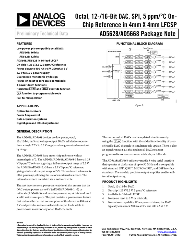
FUNCTIONAL BLOCK DIAGRAM
V R E F IN /V R E F O U T
V DD
AD5628/AD5668
LDAC
1.25V /2.5V
REF
IN P U T
R E G IS T E R
IN P U T
R E G IS T E R
SCLK
SYNC
IN T E R F A C E
L O G IC
D IN
CLR function to programmable code
DAC
R E G IS T E R
DAC
R E G IS T E R
LDAC
S T R IN G
DAC B
IN P U T
R E G IS T E R
DAC
R E G IS T E R
S T R IN G
DAC C
IN P U T
R E G IS T E R
DAC
R E G IS T E R
S T R IN G
DAC D
IN P U T
R E G IS T E R
DAC
R E G IS T E R
S T R IN G
DAC E
IN P U T
R E G IS T E R
DAC
R E G IS T E R
S T R IN G
DAC F
IN P U T
R E G IS T E R
DAC
R E G IS T E R
S T R IN G
DAC G
IN P U T
R E G IS T E R
DAC
R E G IS T E R
S T R IN G
DAC H
BUFFER
V O UTA
BUFFER
V O UTB
BUFFER
V O UTC
BUFFER
V O UTD
BUFFER
V O UTE
BUFFER
V O UTF
BUFFER
V O UTG
BUFFER
V O UTH
P O W E R -D O W N
L O G IC
P O W E R -O N
RESET
Rail-to-rail operation
S T R IN G
DAC A
G ND
CLR
05302-001
Preliminary Technical Data
Octal, 12-/16-Bit DAC, SPI, 5 ppm/°C OnChip Reference in 4mm X 4mm LFCSP
AD5628/AD5668 Package Note
Figure 1.
APPLICATIONS
Optical transceivers
Power Amp control
Data acquisition systems
Digital gain and offset adjustment
GENERAL DESCRIPTION
The AD5628/AD5668 devices are low power, octal,
12-/16-bit, buffered voltage-output DACs. All devices operate
from a single 2.7 V to 5.5 V supply and are guaranteed monotonic
by design.
The AD5628/AD5668 have an on-chip reference with an
internal gain of 2. The AD5628/AD5648/AD5668-1 have a 1.25
V 5 ppm/°C reference, giving a full-scale output range of 2.5 V;
the AD5628/AD5668-2, -3 have a 2.5 V 5 ppm/°C reference,
giving a full-scale output range of 5 V. The on-board reference is
off at power-up, allowing the use of an external reference. The
internal reference is enabled via a software write.
The part incorporates a power-on reset circuit that ensures that the
DAC output powers up to 0 V (AD5628/AD5668-1, -2) or
midscale (AD5668-3) and remains powered up at this level until
a valid write takes place. The part contains a power-down feature
that reduces the current consumption of the device to 400 nA at
5 V and provides software-selectable output loads while in
power-down mode for any or all DAC channels.
Rev PrA
Information furnished by Analog Devices is believed to be accurate and reliable. However, no
responsibility is assumed by Analog Devices for its use, nor for any infringements of patents or other
rights of third parties that may result from its use. Specifications subject to change without notice. No
license is granted by implication or otherwise under any patent or patent rights of Analog Devices.
Trademarks and registered trademarks are the property of their respective owners.
The outputs of all DACs can be updated simultaneously
using the LDAC function, with the added functionality of userselectable DAC channels to simultaneously update. There is also
an asynchronous CLR that updates all DACs to a userprogrammable code—zero scale, midscale, or full scale.
The AD5628/AD5668 utilize a versatile 3-wire serial interface
that operates at clock rates of up to 50 MHz and is compatible
with standard SPI®, QSPI™, MICROWIRE™, and DSP interface
standards. The on-chip precision output amplifier enables railto-rail output swing.
PRODUCT HIGHLIGHTS
1.
2.
3.
4.
5.
Octal, 12-/16-bit DAC.
On-chip 1.25 V/2.5 V, 5 ppm/°C reference.
Available in 16-lead LFCSP.
Power-on reset to 0 V or midscale.
Power-down capability. When powered down, the DAC
typically consumes 200 nA at 3 V and 400 nA at 5 V.
One Technology Way, P.O. Box 9106, Norwood, MA 02062-9106, U.S.A.
www.analog.com
Tel: 781.329.4700
Fax: 781.461.3113
© 2010 Analog Devices, Inc. All rights reserved.
AD5628/AD5668 Package Note
Preliminary Technical Data
13 DIN
10 VOUTD
9
VOUTF
V OUTH 8
VOUT G 5
7
TO P
V IE W
VOUTC 3
VOUT E 4
12 GND
11 VOUTB
00000-000
14 SCLK
AD5668
AD5628
CLR
1
VOUT A 2
VREFIN/V REFOUT 6
V DD
15 LDAC
16 SYNC
PIN CONFIGURATIONS AND FUNCTION DESCRIPTIONS
Figure 2. 16-Lead LFCSP (CP-16-17)
Table 1. Pin Function Descriptions
16-Lead
LFCSP
15
Mnemonic
Description
LDAC
16
SYNC
1
VDD
2
11
3
10
6
VOUTA
VOUTB
VOUTC
VOUTD
VREFIN/VREFOUT
7
CLR
4
9
5
8
12
13
VOUTE
VOUTF
VOUTG
VOUTH
GND
DIN
14
SCLK
Pulsing this pin low allows any or all DAC registers to be updated if the input
registers have new data. This allows all DAC outputs to simultaneously update.
Alternatively, this pin can be tied permanently low.
Active Low Control Input. This is the frame synchronization signal for the input
data. When SYNC goes low, it powers on the SCLK and DIN buffers and enables the
input shift register. Data is transferred in on the falling edges of the next 32 clocks.
If SYNC is taken high before the 32nd falling edge, the rising edge of SYNC acts as an
interrupt and the write sequence is ignored by the device.
Power Supply Input. These parts can be operated from 2.7 V to 5.5 V, and the supply
should be decoupled with a 10 µF capacitor in parallel with a 0.1 µF capacitor to
GND.
Analog Output Voltage from DAC A. The output amplifier has rail-to-rail operation.
Analog Output Voltage from DAC B. The output amplifier has rail-to-rail operation.
Analog Output Voltage from DAC C. The output amplifier has rail-to-rail operation.
Analog Output Voltage from DAC D. The output amplifier has rail-to-rail operation.
The AD5628/AD5648/AD5668 have a common pin for reference input and
reference output. When using the internal reference, this is the reference output
pin. When using an external reference, this is the reference input pin. The default
for this pin is as a reference input.
Asynchronous Clear Input. The CLR input is falling edge sensitive. When CLR is low,
all LDAC pulses are ignored. When CLR is activated, the input register and the DAC
register are updated with the data contained in the CLR code register—zero,
midscale, or full scale. Default setting clears the output to 0 V.
Analog Output Voltage from DAC E. The output amplifier has rail-to-rail operation.
Analog Output Voltage from DAC F. The output amplifier has rail-to-rail operation.
Analog Output Voltage from DAC G. The output amplifier has rail-to-rail operation.
Analog Output Voltage from DAC H. The output amplifier has rail-to-rail operation.
Ground Reference Point for All Circuitry on the Part.
Serial Data Input. This device has a 32-bit shift register. Data is clocked into the
register on the falling edge of the serial clock input.
Serial Clock Input. Data is clocked into the input shift register on the falling edge of
the serial clock input. Data can be transferred at rates of up to 50 MHz.
Rev. PrA | Page 2 of 4
Preliminary Technical Data
AD5628/AD5668 Package Note
OUTLINE DIMENSION
PIN 1
INDICATOR
4.10
4.00 SQ
3.90
0.35
0.30
0.25
0.65
BSC
16
13
PIN 1
INDICATOR
12
1
EXPOSED
PAD
4
2.70
2.60 SQ
2.50
9
0.45
0.40
0.35
TOP VIEW
0.80
0.75
0.70
5
8
0.25 MIN
BOTTOM VIEW
SEATING
PLANE
012909-B
0.05 MAX
0.02 NOM
COPLANARITY
0.08
0.20 REF
COMPLIANT TO JEDEC STANDARDS MO-220-WGGC.
Figure 2. 16-Lead Frame Chip Scale Package [LFCSP]
(CP-16-17)
Dimensions shown in millimeters
ORDERING GUIDE
Model
AD5628ACPZ-1
AD5628ACPZ-2
AD5628BCPZ-2
AD5668ACPZ-2
AD5668ACPZ-3
AD5668BCPZ-1
AD5668BCPZ-2
EVAL-AD5668EBZ-CP
Temperature Range
−40°C to +105°C
−40°C to +105°C
−40°C to +105°C
−40°C to +105°C
−40°C to +105°C
−40°C to +105°C
−40°C to +105°C
Package Description
16-Lead LFCSP
16-Lead LFCSP
16-Lead LFCSP
16-Lead LFCSP
16-Lead LFCSP
16-Lead LFCSP
16-Lead LFCSP
LFCSP Evaluation board
©2010 Analog Devices, Inc. All rights reserved. Trademarks and
registered trademarks are the property of their respective owners.
Rev. PrA | Page 3 of 4
Package
Option
CP-16-17
CP-16-17
CP-16-17
CP-16-17
CP-16-17
CP-16-17
CP-16-17
Power-On
Reset to Code
Zero
Zero
Zero
Zero
Midscale
Zero
Zero
Accuracy
±2 LSB INL
±2 LSB INL
±1 LSB INL
±32 LSB INL
±32 LSB INL
±16 LSB INL
±16 LSB INL
Internal
Reference
1.25V
2.5V
2.5V
2.5V
2.5V
1.25V
2.5V
AD5628/AD5668 Package Note
Preliminary Technical Data
Rev. PrA | Page 4 of 4

