ARTICLE IN PRESS
Microelectronics Journal 40 (2009) 185–192
Contents lists available at ScienceDirect
Microelectronics Journal
journal homepage: www.elsevier.com/locate/mejo
Application of a combined methodology for extraction of the electrical model
of a lead frame chip-scale package
Eoin Mc Gibney , John Barrett
Department of Electronic Engineering, Centre for Adaptive Wireless Systems, Cork Institute of Technology, Bishopstown, Cork, Ireland
a r t i c l e in fo
abstract
Article history:
Received 25 March 2008
Accepted 15 July 2008
Available online 30 August 2008
An ultra-miniature interconnect (IC) package such as a chip-scale package (CSP) provides a difficult
challenge in electrical model extraction, particularly to multi-GHz frequencies, because the very small
parasitics can easily be swamped by test fixture parasitics and/or by small measurement errors that
might be negligible in a larger package. Incomplete data for the high-frequency electrical properties of
package materials and small dimensional errors in physical model entry into electromagnetic (EM)
simulators, again negligible in larger packages, may also cause significant error. Therefore, for ultraminiature packages it is necessary to cross-correlate multiple measurement and simulation methods to
ensure that an accurate package electrical model is obtained. This paper therefore presents a closedloop cross-correlation of s-parameter and time domain reflectometry (TDR) measurements with EM
simulation and TDR simulation for a 16-pin lead frame chip-scale package (LFCSP) and the extraction of
a cross-verified electrical model to 10 GHz. The authors are not aware of the previous application of
these multiple techniques to a CSP to this bandwidth.
& 2008 Elsevier Ltd. All rights reserved.
Keywords:
Electrical modeling
IC packaging
Equivalent circuit extraction
s-parameter measurement
Time domain reflectometry
1. Introduction
There are a variety of reported methodologies for the
characterisation of electrically short interconnects, in particular
IC packaging [1–7]. These methodologies include:
(a)
(b)
(c)
(d)
(e)
low-frequency (DC) measurements (LCR meter),
high-frequency s-parameter measurement,
time domain reflectometry (TDR) techniques,
electromagnetic (EM) simulation,
analytical analysis.
In general, experimental measurement approaches to IC
package modeling rely on the measurement of the package
response to a certain excitation and the fitting, by means of
optimisation, of the simulated response of a proposed equivalent
circuit to best match the measured response. This technique has
one immediate drawback: if the circuit response is fitted to only
one data set, then any inaccuracies due to the measurement
procedure can be incorporated into the equivalent circuit model
during the fitting procedure. This can particularly be of issue
when measuring ultra-miniature packaging and interconnects at
high frequency where a high degree of measurement repeatability
Corresponding author. Tel.: +353 868 780 885.
E-mail address: eoin.mcgibney@analog.com (E. Mc Gibney).
0026-2692/$ - see front matter & 2008 Elsevier Ltd. All rights reserved.
doi:10.1016/j.mejo.2008.07.004
and minimal measurement error can be difficult to ensure.
Additionally, the extraction of an accurate model using EM
simulation alone can also be challenging. Inaccurate material
parameters at high frequencies, tolerances of physical dimensions
and the type of 3D EM solver and its method of application heavily
influence the simulation outcomes. Therefore, to provide a highconfidence level, extracted equivalent circuit models have to be
validated/correlated. This can be done using further experimental
measurement and EM simulation or as proposed in this paper—
a combination of both. Therefore, a closed-loop electrical modeling methodology that cross-correlates two methods of package
measurement with two methods of package simulation has been
used in the work described in this paper.
2. Previous work and methodology
The application of electrical characterisation techniques in
combination is rarely performed; it is typical for modeling
approaches to be applied in isolation. Previous published research
by Horng et al. [8] has compared the application of frequency
and time domain measurement techniques for the electrical
modeling of a 388 lead plastic ball grid array. s-parameter
measurements (30 kHz–6 GHz frequency range) and TDR measurements were taken on selected package interconnects. Equivalent circuit models, consisting of transmission line elements, were
developed and compared. The main observations made by the
ARTICLE IN PRESS
186
E. Mc Gibney, J. Barrett / Microelectronics Journal 40 (2009) 185–192
3D EM Simulations
- Full wave solver
- Quasi-static solver
Measurement Set-up
-Sample Preparation
- Test Fixture Mfg.
Frequency and Time Domain
Measurement
- Calibration/De-embedding
Iterative Loop
Mechanical Drawings
-Package Leadframe
-Test Fixture
Material Properties
- Er, tan d
Equialent Circuit
Selection
- Electrical length
- Bandwidth
Equivalent Circuit Extraction
-Initial circuit element extraction
-Optimisation
Model Validation
Good Agreement
between Model and
Measurement
No
Yes
Validated equivalent circuit
model for IC package
Fig. 1. Design flow for modeling methodology.
authors were: (1) a frequency domain approach typically has
better resolution in determining circuit parameters. (2) Frequency
domain approaches support better calibration methods and
therefore more accurate measurements can be made and (3)
TDR offers faster measurements but it does not offer the same
resolution. The authors also propose a strategy in which a TDR
method may be used to extract an initial model and this model
may then be refined using optimisation and fitting to frequency
domain data. The author’s underlying conclusion is that a
combination of both techniques could extract the equivalent
coupled transmission line model with the widest bandwidth.
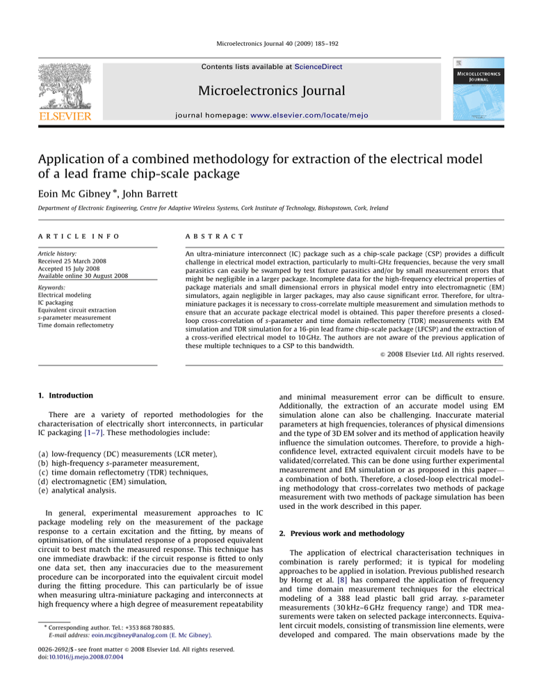
The modeling methodology implemented in this work combines s-parameter and TDR/transmission (TDR/T) measurements
with both 3D EM simulation and TDR simulation. The steps taken
are illustrated in the flow chart shown in Fig. 1. It can be seen that
the flow has an iterative ‘loop’ that terminates when an accurate
and validated high-frequency circuit model is obtained. A general
approach for the high-frequency measurement of IC packaging
parasitics was used in the experimental characterisation process.
This method, based on multiconductor modeling, has been
previously reported in [2,7,9]. It was chosen both for its suitability
for modeling electrically short interconnects and implementation
using a vector network analyser (VNA) [9]. For accurate electrical
measurement of the package and to ensure repeatability of
measurements, a custom measurement fixture was designed.
The parasitic effects of this fixture were removed using a
de-embedding procedure to obtain s-parameters for the IC
package alone. The resulting s-parameters, measured up to
15 GHz, are used to calculate circuit element values for a firstestimate lumped element equivalent circuit. The lumped element
values are then optimised using a circuit simulator to fit the
equivalent circuit response with that of the de-embedded
s-parameters over frequency. To experimentally validate the
extracted circuit model, two-port TDR was used to measure
the reflected voltage, near-end crosstalk and even/odd mode
responses of the lead frame chip-scale package (LFCSP). These
are compared with TDR simulations of the equivalent circuit
model using SPICE. The correlation between the measured and
simulated responses is used as the terminating criterion for the
modeling methodology. The 42 ps input step risetime of the TDR
ID
547875
Title
Applicationofacombinedmethodologyforextractionoftheelectricalmodelofaleadframechip-scale
package
http://fulltext.study/article/547875
http://FullText.Study
Pages
8


