GP2S24J0000F Series
GP2S24J0000F
Series
Detecting Distance : 0.7mm
Phototransistor Output,
Compact Reflective
Photointerrupter
■ Description
■ Agency approvals/Compliance
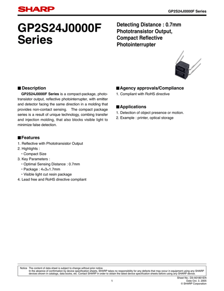
GP2S24J0000F Series is a compact-package, phototransistor output, reflective photointerrupter, with emitter
and detector facing the same direction in a molding that
provides non-contact sensing. The compact package
series is a result of unique technology, combing transfer
and injection molding, that also blocks visible light to
minimize false detection.
1. Compliant with RoHS directive
■ Applications
1. Detection of object presence or motion.
2. Example : printer, optical storage
■ Features
1. Reflective with Phototransistor Output
2. Highlights :
• Compact Size
3. Key Parameters :
• Optimal Sensing Distance : 0.7mm
• Package : 4×3×1.7mm
• Visible light cut resin package
4. Lead free and RoHS directive compliant
Notice The content of data sheet is subject to change without prior notice.
In the absence of confirmation by device specification sheets, SHARP takes no responsibility for any defects that may occur in equipment using any SHARP
devices shown in catalogs, data books, etc. Contact SHARP in order to obtain the latest device specification sheets before using any SHARP device.
1
Sheet No.: D3-A01801EN
Date Oct. 3. 2005
© SHARP Corporation
GP2S24J0000F Series
■ Internal Connection Diagram
4
3
1
2
3
4
1
2
(Unit : mm)
(0.4) Detector center
(0.2) Emitter center
■ Outline Dimensions
Top view
4
Anode
Emitter
Collector
Cathode
3
C0.7
1
2
1.75
∗4±0.2
3+0.2
−0.1
0.75
1.7
4+0.2
−0.1
3.5+1
−0
4−(0.5)
4−0.15+0.2
−0.1
4−0.4+0.2
−0.1
(4)
±15°
Date
code
mark
θ
θ : 0 to 20°
• Tolerance : ±1.5mm
• ( ) : Reference dimensions
• The dimensions indicated by ∗ refer
to those measured from the lead
bending part.
• The dimensions shown do not include
burr.
Burr's dimension : 0.15mm MAX.
Product mass : approx. 0.04g
Plating material : SnCu (Cu : TYP. 2%)
Sheet No.: D3-A01801EN
2
GP2S24J0000F Series
Date code (Symbol)
January
July
February
August
March
September
April
October
May
November
June
December
Rank mark
There is no rank indicator.
Country of origin
Japan
Sheet No.: D3-A01801EN
3
■ Absolute Maximum Ratings
Parameter
Forward current
Input Reverse voltage
Power dissipation
Collector-emitter voltage
Emitter-collector voltage
Output
Collector current
Collector power dissipation
Total power dissipation
Operating temperature
Storage temperature
∗1
Soldering temperature
∗
Symbol
Rating
IF
50
VR
6
P
75
VCEO
35
VECO
6
20
IC
75
PC
100
Ptot
Topr
−25 to +85
Tstg
−40 to +100
Tsol
260
(Ta=25˚C)
Unit
mA
V
mW
V
V
mA
mW
mW
˚C
˚C
˚C
1mm or more
GP2S24J0000F Series
Soldering area
1 For 5s or less
■ Electro-optical Characteristics
Parameter
Forward voltage
Input
Reverse current
Output Collector dark current
∗2
Collector Current
Transfer
Rise time
Response time
characFall time
teristics ∗3
Leak current
∗
∗
Symbol
VF
IR
ICEO
IC
tr
tf
ILEAK
Condition
IF=20mA
VR=6V
VCE=20V
IF=4mA, VCE=2V
VCE=2V, IC=100μA,
RL=1kΩ, d=1mm
IF=4mA, VCE=2V
MIN.
−
−
−
20
−
−
−
TYP.
1.2
−
1
45
20
20
−
(Ta=25˚C)
MAX.
Unit
1.4
V
10
μA
100
nA
120
μA
100
μs
100
100
nA
2 The condition and arrangement of the reflective object are shown below.
The rank splitting of collector current (IC) shall be executed according to the table below.
Rank
Collector current, IC [μA]
(IF=4mA, VCE=2V)
A
20 to 42
Yellow
B
34 to 71
Transparent
C
58 to 120
Green
Package sleeve color
3 Without reflective object.
● Test Conditon and Arrangement for Collector Current
Al evaporation
d=1mm glass plate
Sheet No.: D3-A01801EN
4
GP2S24J0000F Series
■ Model Line-up
∗
Model No.
Rank
GP2S24J0000F
GP2S24BJ000F
GP2S24CJ000F
GP2S24ABJ00F
GP2S24BCJ00F
A, B or C
B
C
A or B
B or C
Collector current IC[μA]
(IF=4mA, VCE=2V, Ta=25˚C)
20 to 120
34 to 71
58 to 120
20 to 71
34 to 120
The ratio of each rank can not be guaranteed.
Please contact a local SHARP sales representative to inquire about production status.
Sheet No.: D3-A01801EN
5
GP2S24J0000F Series
Fig.2 Power Dissipation vs.
Ambient Temperature
60
120
50
100
Power dissipation P (mW)
Forward current IF (mA)
Fig.1 Forward Current vs. Ambient
Temperature
40
30
20
Ptot
P, PC
80
75
60
40
20
15
10
0
−25
0
25
50
75
Ambient temperature Ta (˚C)
85
0
−25
100
VCE =2V
Ta =25˚C
600
0˚C
−25˚C
Collector current IC (μA)
Forward current IF (mA)
700
100
100
Fig.4 Collector Current vs.
Forward Current
Fig.3 Forward Current vs. Forward
Voltage
Ta =75˚C
50˚C
25˚C
50
75 85
0
25
Ambient temperature Ta (˚C)
10
500
400
300
200
100
1
0
0.5
1
1.5
2
Forward voltage VF (V)
2.5
0
3
0
Fig.5 Collector Current vs.
Collector-Emitter Voltage
Ta =
25˚C
Collector current IC (μA)
300
120
IF =15mA
250
10mA
200
150
10
15
20
Forward current IF (mA)
25
30
Fig.6 Relative Collector Current vs.
Ambient Temperature
Relative collector current IC (%)
350
5
7mA
100
4mA
50
IF =4mA
VCE =2V
100
80
60
40
20
2mA
0
0
2
4
6
8
10
Collector-emitter voltage VCE (V)
0
−25
12
0
25
50
75
Ambient temperature Ta (˚C)
100
Sheet No.: D3-A01801EN
6
GP2S24J0000F Series
Fig.7 Collector Dark Current vs.
Ambient Temperature
1 000
VCE =20V
VCE=2V
IC=100μA
Ta=25˚C
10 −8
tf
td
10
ts
1
10 −9
10 −10
0
0.1
0.1
100
25
50
75
Ambient temperature Ta (˚C)
1
Input
Output
Relative collector current (%)
RD
VCC
RL
100
1 000
Fig.10 Relative Collector Current vs.
Distance (Reference value)
100
Reflector
Plate
10
Load resistance RL (kΩ)
Fig.9 Test Circuit for Response Time
Input
tr
100
10 −7
Response time (μs)
Collector dark current ICEO (A)
10 −6
Fig.8 Response Time vs. Load
Resistance
10%
Output
90%
td
tr
ts
tf
IF =4mA
VCE =2V
Ta =25˚C
80
60
40
20
0
0
1
2
3
4
5
Distance between sensor and Al evaporation glass d (mm)
Fig.11 Detecting Position Characteristics (1)
Fig.12 Detecting Position Characteristics (2)
100
IF=4mA
VCE=2V
d=1mm
Ta=25˚C
80
Relative collector current (%)
Relative collector current (%)
100
60
40
20
0
−2
−1
0
1
2
3
4
5
6
80
60
40
20
0
−3
7
Card moving distance L (mm)
IF=4mA
VCE=2V
d=1mm
Ta=25˚C
−2
−1
1
3
0
2
4
Card moving distance L (mm)
5
6
Sheet No.: D3-A01801EN
7
GP2S24J0000F Series
Fig.13 Test Condition for Distance &
Detecting Position Characteristics
Fig.14 Freauency Response
5
Al evaporated glass
Correspond to Fig.10
VCE =2V
IC =100μA
Ta =25˚C
d
Correspond to Fig.11
Correspond to Fig.12
Test condition
IF = 4mA
VCE = 2V
d = 1mm
Test condition
IF = 4mA
VCE = 2V
d = 1mm
OMS card
White
OMS card
Black
d
1mm
−
L=0
Voltage gain AV (dB)
0
Black
White
d
+
L=0
1kΩ
RL =10kΩ
−10
−15
1mm
−
−5
-20
102
103
104
Frequency f (Hz)
105
106
+
Fig.15 Spectral Sensitivity (Detecting Side)
100
Ta=25˚C
Relative sensitivity (%)
80
60
40
20
0
600
700
800
900
1 000
Wavelength λ (nm)
1 100
1 200
Remarks : Please be aware that all data in the graph are just for reference and not for guarantee.
Sheet No.: D3-A01801EN
8
GP2S24J0000F Series
■ Design Considerations
● Design guide
1) Prevention of detection error
To prevent photointerrupter from faulty operation caused by external light, do not set the detecting face to
the external light.
2) Distance characteristic
Please refer to Fig.10 (Relative collector current vs. Distance) to set the distance of the photointerrupter
and the object.
This product is not designed against irradiation and incorporates non-coherent IRED.
● Degradation
In general, the emission of the IRED used in photointerrupter will degrade over time.
In the case of long term operation, please take the general IRED degradation (50% degradation over 5
years) into the design consideration.
● Parts
This product is assembled using the below parts.
• Photodetector (qty. : 1)
Category
Material
Maximum Sensitivity
wavelength (nm)
Sensitivity
wavelength (nm)
Response time (μs)
Phototransister
Silicon (Si)
930
700 to 1 200
20
• Photo emitter (qty. : 1)
Category
Material
Maximum light emitting
wavelength (nm)
I/O Frequency (MHz)
Infrared emitting diode
(non-coherent)
Gallium arsenide (GaAs)
950
0.3
• Material
Case
Lead frame
Lead frame plating
Black polyphernylene
42Alloy
SnCu plating
Sheet No.: D3-A01801EN
9
GP2S24J0000F Series
■ Manufacturing Guidelines
● Soldering Method
Flow Soldering:
Soldering should be completed below 260˚C and within 5 s.
Soldering area is 1mm or more away from the bottom of housing.
Please take care not to let any external force exert on lead pins.
Please don't do soldering with preheating, and please don't do soldering by reflow.
Other notice
Please test the soldering method in actual condition and make sure the soldering works fine, since the
impact on the junction between the device and PCB varies depending on the cooling and soldering
conditions.
● Cleaning instructions
Solvent cleaning :
Solvent temperature should be 45˚C or below. Immersion time should be 3 minutes or less.
Ultrasonic cleaning :
Do not execute ultrasonic cleaning.
Recommended solvent materials :
Ethyl alcohol, Methyl alcohol and Isopropyl alcohol.
● Presence of ODC
This product shall not contain the following materials.
And they are not used in the production process for this product.
Regulation substances : CFCs, Halon, Carbon tetrachloride, 1.1.1-Trichloroethane (Methylchloroform)
Specific brominated flame retardants such as the PBBOs and PBBs are not used in this product at all.
This product shall not contain the following materials banned in the RoHS Directive (2002/95/EC).
•Lead, Mercury, Cadmium, Hexavalent chromium, Polybrominated biphenyls (PBB), Polybrominated
diphenyl ethers (PBDE).
Sheet No.: D3-A01801EN
10
GP2S24J0000F Series
■ Package specification
● Sleeve package
Package materials
Sleeve : Polystyrene
Stopper : Styrene-Butadiene
Package method
MAX. 50 pcs. of products shall be packaged in a sleeve. Both ends shall be closed by tabbed and tabless
stoppers.
MAX. 40 sleeves in one case.
Color of sleeve
Rank classification is distinguished by the color of the sleeve as shown in the table below.
But the ratio of each rank can not be guaranteed.
Rank
A
B
C
Color of sleeve
Yellow
Transparent
Green
Sheet No.: D3-A01801EN
11
GP2S24J0000F Series
■ Important Notices
· The circuit application examples in this publication
are provided to explain representative applications of
SHARP devices and are not intended to guarantee any
circuit design or license any intellectual property rights.
SHARP takes no responsibility for any problems related
to any intellectual property right of a third party resulting
from the use of SHARP's devices.
with equipment that requires higher reliability such as:
--- Transportation control and safety equipment (i.e.,
aircraft, trains, automobiles, etc.)
--- Traffic signals
--- Gas leakage sensor breakers
--- Alarm equipment
--- Various safety devices, etc.
(iii) SHARP devices shall not be used for or in
connection with equipment that requires an extremely
high level of reliability and safety such as:
--- Space applications
--- Telecommunication equipment [trunk lines]
--- Nuclear power control equipment
--- Medical and other life support equipment (e.g.,
scuba).
· Contact SHARP in order to obtain the latest device
specification sheets before using any SHARP device.
SHARP reserves the right to make changes in the
specifications, characteristics, data, materials, structure,
and other contents described herein at any time
without notice in order to improve design or reliability.
Manufacturing locations are also subject to change
without notice.
· If the SHARP devices listed in this publication fall
within the scope of strategic products described in the
Foreign Exchange and Foreign Trade Law of Japan, it
is necessary to obtain approval to export such SHARP
devices.
· Observe the following points when using any devices
in this publication. SHARP takes no responsibility for
damage caused by improper use of the devices which
does not meet the conditions and absolute maximum
ratings to be used specified in the relevant specification
sheet nor meet the following conditions:
(i) The devices in this publication are designed for use
in general electronic equipment designs such as:
--- Personal computers
--- Office automation equipment
--- Telecommunication equipment [terminal]
--- Test and measurement equipment
--- Industrial control
--- Audio visual equipment
--- Consumer electronics
(ii) Measures such as fail-safe function and redundant
design should be taken to ensure reliability and safety
when SHARP devices are used for or in connection
· This publication is the proprietary product of SHARP
and is copyrighted, with all rights reserved. Under
the copyright laws, no part of this publication may be
reproduced or transmitted in any form or by any means,
electronic or mechanical, for any purpose, in whole or in
part, without the express written permission of SHARP.
Express written permission is also required before any
use of this publication may be made by a third party.
· Contact and consult with a SHARP representative
if there are any questions about the contents of this
publication.
Sheet No.: D3-A01801EN
[H143]
12
