Design of Ultra Low Dropout Voltage Boost Converter
advertisement
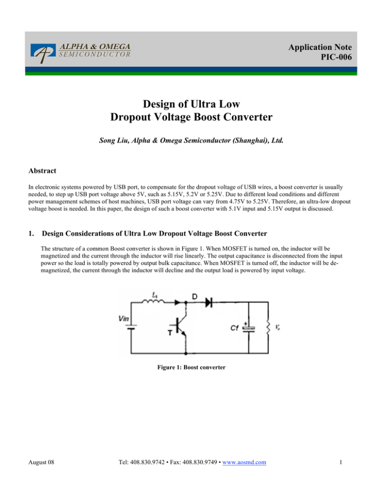
Application Note PIC-006 Design of Ultra Low Dropout Voltage Boost Converter Song Liu, Alpha & Omega Semiconductor (Shanghai), Ltd. Abstract In electronic systems powered by USB port, to compensate for the dropout voltage of USB wires, a boost converter is usually needed, to step up USB port voltage above 5V, such as 5.15V, 5.2V or 5.25V. Due to different load conditions and different power management schemes of host machines, USB port voltage can vary from 4.75V to 5.25V. Therefore, an ultra-low dropout voltage boost is needed. In this paper, the design of such a boost converter with 5.1V input and 5.15V output is discussed. 1. Design Considerations of Ultra Low Dropout Voltage Boost Converter The structure of a common Boost converter is shown in Figure 1. When MOSFET is turned on, the inductor will be magnetized and the current through the inductor will rise linearly. The output capacitance is disconnected from the input power so the load is totally powered by output bulk capacitance. When MOSFET is turned off, the inductor will be demagnetized, the current through the inductor will decline and the output load is powered by input voltage. Figure 1: Boost converter August 08 Tel: 408.830.9742 • Fax: 408.830.9749 • www.aosmd.com 1 Application Note PIC-006 When MOSFET is turned on, the equation is below: And then . When MOSFET is turned off and take the dropout voltage of the diode, the equation is below: So The equation below can be deduced: For , , , it can be calculated: For peak current mode, there is a leading edge blanking time for current sense signal. This determines the minimum PWM on time.(1) This value is between 100~200nS and usually 150ns is selected for tolerance consideration. If the boost converter operates at 1MHz switching frequency, the on time from 5.1V to 5.15V is equal to =81nS. This value is less than the minimum PWM on time, which is 150nS. As a result, the converter will skip some pulses and enter into pulse skipping mode.(2) At this mode, output voltage ripple is high, which interferes with the normal operation of the complete system, causing EMI issues and so on. In some critical conditions, it will make the downstream circuits with low voltage ratings to fail. 2. Solution for Ultra Low Dropout Voltage Boost Converter The minimum on time is one of intrinsic characteristics of PWM and determined by leading edge blanking time. From the equation: It can be found that increasing the duty cycle or decreasing switching frequency can increase MOSFET on time at maximum input voltage. Note that at maximum input voltage, MOSFET on time is minimal. If actual minimal on time at maximum input voltage is more than the minimum PWM on time, the system cannot go into pulse skipping mode so the output voltage is always under strict regulation. If the switching frequency can be set externally, PWM can work in relatively low switching frequency to avoid above issue. But at low switching frequency, larger output capacitors and inductors with high cost and more board area are needed. It is not practical in many portable systems. Furthermore, in order to reduce pin count, the switching frequency of most of monolithic boost converter is fixed internally. Other methods are adopted because the switching frequency is not adjusted externally. August 08 Tel: 408.830.9742 • Fax: 408.830.9749 • www.aosmd.com 2 Application Note PIC-006 The duty cycle is calculated by the below equation: . From it, it is very obvious that increasing the value of can increase the duty cycle, as shown in Figure 2. Figure 2: The boost converter with an additional diode At this condition, duty cycle is: 。 Similarly, , , , ,it can be calculated: 。 From the calculation above, when a series diode is added, the duty cycle is increased form 8.1 to 14.3. Its drawbacks are that it requires an additional component and decreases the efficiency of the system. It is also true that increasing the output voltage a little higher can increase the duty cycle. However, high output will impose the over voltage risk on the downstream circuits or ICs. This method is not recommended in this application. 3. Conclusion The minimum duty cycle of PWM can be increased with an external diode in series, which prevents the system from going into skip pulse mode. However, this diode will increase power dissipation, resulting in lower efficiency. Reference (1) Song Liu, Design Tips for Buck Converter in Automobile Electronic System, Electronic Design and Application, 2007, (5): 111 ~ 114. (2) Song Liu, The Principle and Application of Three Operation Modes of Buck Converter at Light Load, Power Electronics, 2007, 41(11): 75 ~ 76. Copyright © 2008 Alpha & Omega Semiconductor, Inc. August 08 Tel: 408.830.9742 • Fax: 408.830.9749 • www.aosmd.com 3
