Circuit for LPI signal detection and suppression of conventional
advertisement
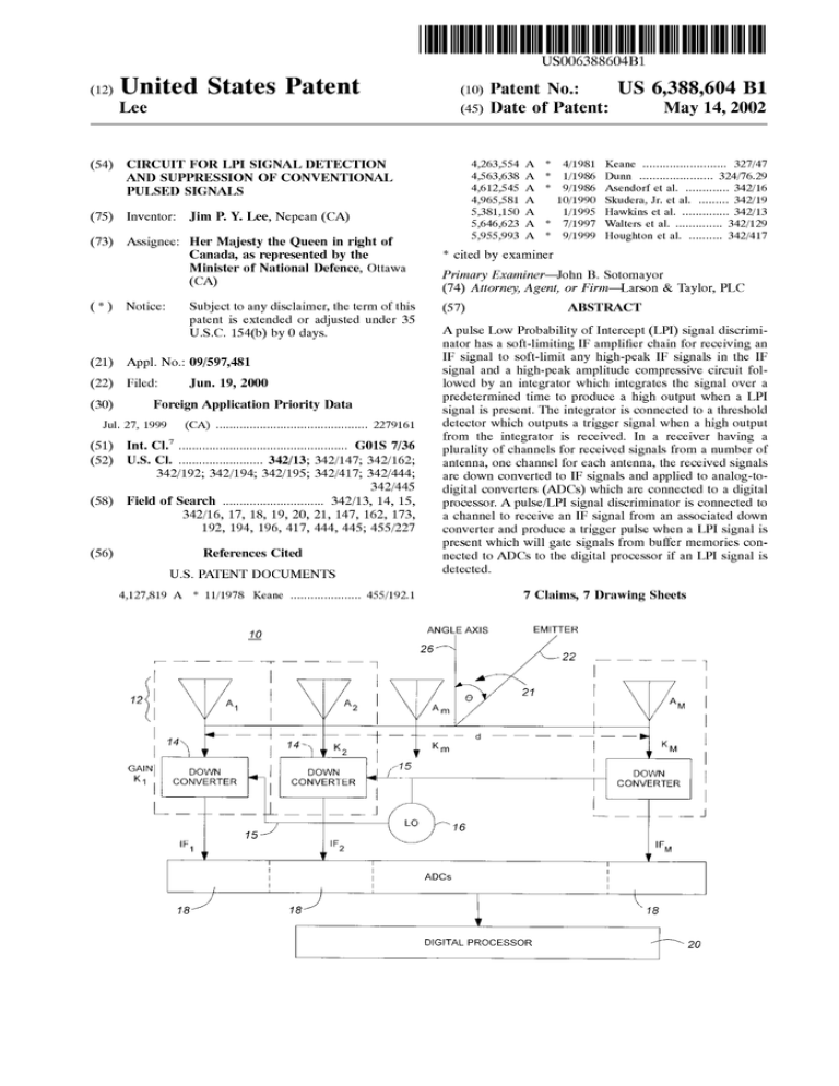
US006388604B1 (12) United States Patent (10) Patent N0.: US 6,388,604 B1 (45) Date of Patent: May 14, 2002 Lee (54) CIRCUIT FOR LPI SIGNAL DETECTION 4,263,554 A * 4/1981 Keane ....................... .. 327/47 AND SUPPRESSION ()F CONVENTIONAL PULSED SIGNALS 4,563,638 A 4,612,545 A * * 1/1986 Dunn .................... .. 324/76.29 9/1986 Asendorf et al. ........... .. 342/16 4,965,581 A _ - 5,381,150 A (75) Inventor‘ (73) Assigneez Her Majesty the Queen in right of (*) J ‘m P‘ Y‘ Lee’ Nepean (CA) Notice: ( ) (22) A (74) Attorney, Agent, or Firm—Larson & Taylor, PLC (57) ABSTRACT (51) (52) Apulse LoW Probability of Intercept (LPI) signal discrimi nator has a soft-limiting IF ampli?er chain for receiving an IF signal to soft-limit any high-peak IF signals in the IF / ’ Jun. 19, 2000 _ signal and a high-peak amplitude compressive circuit fol loWed by an integrator Which integrates the signal over a _ _ _ predetermined time to produce a high output When a LPI Forelgn Apphcatlon Pnonty Data Jul. 27, 1999 signal is present. The integrator is connected to a threshold (CA) ........................................... .. 2279161 detector Which Outputs a trigger signal When a high Output from the integrator is received. In a receiver having a plurality of Channels for received Signals from a number of antenna, one channel for each antenna, the received signals 7 Int. Cl. ................................................ .. G018 7/36 US Cl- ~~~~~~~~~~~~~~~~~~~~~~~ ~~ 342/13; 342/147; 342/162; 342/192; 342/194; 342/195; 342/417; 342/444; (58) 7/1997 Walters et al. ............ .. 342/129 9/1999 Houghton et al. ........ .. 342/417 Primary Examiner—John B. Sotomayor _ (30) 5,646,623 A * 5,955,993 A * gggster 0f Natlonal Defence’ Ottawa Subject to any disclaimer, the term of this patent is extended or adjusted under 35 0 are doWn converted to IF signals and applied to analog-to 342/445 Field Of Search ............................ .. 342/13, 14, 15, 342/16, 17, 18, 19, 20, 21, 147, 162, 173, (56) digital converters (ADCs) Which are connected to a digital processor_ A pulse/LPI Signal discriminator is connected to a channel to receive an IF signal from an associated doWn 192, 194, 196, 417, 444, 445; 455/227 converter and produce a trigger pulse When a LPI signal is _ References Clted present Which Will gate signals from buffer memories con nected to ADCs to the digital processor if an LPI signal is detected. US. PATENT DOCUMENTS 4,127,819 A 342/19 Hawkins et al. ............ .. 342/13 * cited by examiner l. N .._ 09 597 481 pp Filed: 1/1995 Canada, as represented by the USC 154(k)) by 0 days_ 21 10/1990 Skudera, Jr. et al. .. * 11/1978 Keane ................... .. 455/192.1 m 7 Claims, 7 Drawing Sheets ANGLE AXIS EMITTER 26 4 r ~ — — i ~r ‘i 12 I 1 | — — g 22 7 I I A1 i k 1 I A2 I I | i w A i I i 21 A'“ m I l /A l M I | l I l GA'Nl K1 I Fm 14\ muff it l l DOWN l CONVERTER I 14\ l K 2 _ T15 I DOWN 2E K 22__i1__ d m \ K75 CONVERTER l I ‘ I I > KM I r | DOWN I CONVERTER l L_ __ iii_1 Liii_1 15 16 |F1 IF | 18 IFM l l l l l 18j ADCs I DIGITAL PROCESSOR .8 “20 U.S. Patent 1.5 May 14, 2002 Sheet 1 0f 7 US 6,388,604 B1 - PULSED SIGNAL 22 m6an5ti0s?2 O _ f 24 THRESHOLD LEVEL 5.O LPI SIGNAL 20 -O.5 - 10 TIME (us) FIG. 1 12 U.S. Patent May 14, 2002 Sheet 3 0f 7 US 6,388,604 B1 om / a / mm mm mm QR fwm mm OJIwmMF //mm MM.PDOnF wmOk EMO A OM5301<6 cw U.S. Patent May 14, 2002 Sheet 5 0f 7 US 6,388,604 B1 INPUT SIGNAL TO SDLVA Q6 2 0.01 g ‘0-01 I | I I I I I O 2 4 6 8 1O 12 I 14 I I | 16 18 20 VIDEO SIGNAL FROM SDLVA 68 01 V0LTS 0.05 I O I 2 I I I I I I 4 6 8 1O 12 14 INTEGRATOR OUTPUT V0LTS VOLTS '0 '01 | I 01 I 16 I I 18 20 70 U.S. Patent May 14, 2002 Sheet 6 6f 7 US 6,388,604 B1 ~10 — -20 - O Vth = -150 mV X Vth I —3OO mV -3O — + Vth = -600 mV (LPIEONdVWBUmLRT) 400 I I I I I I PULSE WIDTH (us) FIG. 6 I I | I U.S. Patent May 14, 2002 Sheet 7 0f 7 US 6,388,604 B1 -20 — —3O — 0 WITH NO VIDEO LOG AMP 9K WITH VIDEO LOG AMP LPI(NEOdVWBUmTLR) '100 I | I l I l PULSE WIDTH (us) FIG. 7 I I | l US 6,388,604 B1 1 2 CIRCUIT FOR LPI SIGNAL DETECTION AND SUPPRESSION OF CONVENTIONAL PULSED SIGNALS pulsed signals is an interferometer. In an interferometer, a number of antenna elements are distributed in a tWo dimensional plane and phase comparison betWeen different antenna elements is used to determine the AOA. MicroWave This invention relates to a digital system that is used to phase detectors are typically used for phase comparison. detect loW peak power LoW Probability of Intercept (LPI) signals and to suppress strong conventional pulsed signals, Recently these phase detectors have been replaced by digital measurement techniques. The signal characteristics of the intercepted signals are measured either from the output of and more particularly, to such a system Which utiliZes an LPI one of the interferometer antennas or from a separate Discriminator. 10 antenna. Signal characteriZation is performed using an intra BACKGROUND OF THE INVENTION pulse receiver implemented by analog devices. In this case, Various reconnaissance systems are used to intercept radar signals and decipher some of their critical character istics and angles of arrival. A microWave intercept receiver may be used for just this purpose. In particular reconnais a frequency discriminator is used for frequency measure ment While a Detector Log Video Ampli?er (DLVA) is used for amplitude measurement. 15 Detection of LPI signals is currently accomplished using a channeliZed receiver instead of an intrapulse receiver. A the sance receiver applications is designed in areas to ful?ll such roles as Electronic such as radar Warfare Warning, channeliZed receiver is typically implemented using either a electronic support measures (ESM), and Electronic Intelli gence (ELINT). In most conventional approaches, the inter cept receiver is designed to perform tWo functions The ?rst function is to measure the signal characteristics of the intercepted signal, and the second is to determine its angle band of microWave ?lters With a detector at the output of each ?lter. Other receivers may be used, such as a time bandWidth in each channel and thus increase the receiver of arrival (AOA) for the purpose of direction ?nding (DF) sensitivity for LPI signal detection. Other architectures such integrating acousto-optic spectrum analyZer and compres sive receiver. The use of a channeliZer Will reduce the noise and location of the radar source. With the proliferation of radar systems and the increasing number of radars employing complex Waveform 25 as correlators are also suitable for LPI signal detection and AOA determination. These correlators are implemented using analog, optical, or digital technology. HoWever, the modulation, it is dif?cult to differentiate and sort the inter AOA determination process is quite different from the cepted radar signals using just the coarse conventional parameters. Typically these coarse parameters include AOA, mation can be extracted. interferometer approach and very limited intrapulse infor carrier frequency, pulse Width (PW), pulse repetition interval As mentioned above, digital signal processing technology (PRI), and scan pattern. Since many radars have similar conventional parameters, ambiguity may occur in both the is used in both the single-channel and the multi-channel receiver architectures. The potential advantages of digital sorting and identi?cation processes. One type of receiver that may be used to precisely measure the conventional parameters as Well as the intra 35 pulse modulation for both sorting and identi?cation pur poses is the intrapulse receiver. HoWever, the use of LoW Probability of Intercept (LPI) radars With loW peak poWer has introduced a further require ment for modem intercept receivers, requiring them to have a much higher sensitivity in order to detect these LPI radar signals. Until recently, almost all radars Were designed to transmit short duration pulses With a high peak poWer. This type of signal is easy to detect using relatively simple, traditional EW intercept receivers making the attacker (radar still quite a challenge for the digital signal processing technology to meet all of the processing requirements if all of the digitiZed data from the Analog-to-Digital Converters (ADCs) are to be processed in or near real-time. 45 source) vulnerable to either antiradiation missiles or Elec tronic Counter Measures (ECM). HoWever, by using LPI techniques it is possible to design a LPI radar that is effective against traditional EW intercept receivers. One of the most important LPI techniques is the use of phase or frequency approaching one. This technique can result in drastic reduc on a pulse-by pulse basis. Acurrent architecture that accomplishes both signal mea surement and accurate AOA determination on conventional It is to be noted that the vast majority of radar signals are of pulsed nature and the duty cycles are relative loW. Therefore, the portion of the digitiZed data set Where the signals are actually present could be quite small in a typical signal environment. Most conventional radars transmit high peak poWer and pulses With pulse Width less than 1 us. HoWever, LPI signals are generally characteriZed by very loW-peak poWer and are of much longer duration. Pulse Widths of LPI signals are expected to be 5 us and longer. DigitiZed IF signals of an LPI signal and a pulsed signal are shoWn in FIG. 1. If a threshold is used on the digitiZed data to reduce the amount of data to be passed on to the processor, Waveform coding to provide transmitting duty cycles tions in peak transmitted poWer While maintaining the required average poWer. Therefore With an increasing number of radars employing complex Waveform modulation in addition to using loW peak poWer LPI signals, it is required that a modern intercept receiver perform the folloWing three basic functions: a) measure and characteriZe conventional pulsed radar signals; b) detect and characteriZe LPI signals; and c) determine the AOA for both conventional pulsed signals and LPI signals. Furthermore, these three functions should be performed on the intercepted signals in a multiple signal environment and receivers are robustness, ?exibility and cost. However, the processing functions can be quite complex and numerous once the IF signals digitiZed. This is especially true in the case of the multi-channel digital receiver architecture. It is the LPI signal Will likely be missed and undetected. 55 It is an object of the present invention to obviate or mitigate the above disadvantages. SUMMARY OF THE INVENTION The present invention seeks to provide a solution to the problem of radar processor overload When LPI signals are present With conventional pulsed signals. An advantage of the present invention is to enhance the detection of Weak LPI signals. Afurther advantage of the present invention is to suppress 65 the presence of high-peak poWer and short-duration conven tional pulsed signals, and to trigger a data buffer for gating digitiZed LPI data to a processor for processing. US 6,388,604 B1 4 3 Although only one channel is shoWn in FIG. 3, each of the receiver channels has the same capabilities. The receiver is In accordance With this invention there is provided an LPI signal discriminator comprising an ampli?er for receiving an incoming IF signal; a signal detector; and a comparator responsive to the output of the signal detector for producing a trigger signal When the detected signal is above a prede capable of intercepting both conventional and LPI signals. HoWever, the digital processor is not capable of analysing all termined threshold. A still further embodiment of the invention provides for a digital receiver for determining parameters of an incoming signal, comprising: one or more receiver channels, each channel including a respective antenna for receiving the incoming signal; a doWn converter for converting the signal to an intermediate frequency (IF) signal; an analog-to-digital 10 of the signals in real time in a typical signal environment. In order to effectively analyse an LPI signal, it is necessary to ignore the conventional signals and focus only on the LPI signals. Therefore an additional circuit is needed to provide an indication that an LPI signal is present in the digitiZed data, and to transfer the digitiZed data to the processor for processing as soon as an LPI signal is detected. Referring to FIG. 3 a LPI detector circuit according to an converter (ADC) operatively coupled to receive the IF signal embodiment of the present invention is shoWn generally by and to provide a digital signal output in response to a trigger numeral 50. The circuit 50 includes tWo or more IF ampli signal, the digital signal being indicative of the phase and ?ers 52 cascaded With pads betWeen the ampli?ers. This arrangement is used to distribute the signal poWer evenly throughout the chain and to soft limit strong received pulsed signals. The IF ampli?ed signal is detected by a large amplitude of the received signal in the channel; a digital processor operatively coupled to receiving the digital signals from each of the plurality of channels and for determining the parameters by utiliZing the phase and amplitude on a pulse by pulse basis; and an LPI signal discriminator opera tively coupled to the doWn converter for producing the trigger signal When the incoming signal is above a prede termined threshold, to thereby transfer the digitiZed signal to the signal processor for processing the incoming LPI signal. 25 BRIEF DESCRIPTION OF THE DRAWINGS An embodiment of the invention Will noW be described by Way of eXample only, With reference to the accompanying draWings in Which: Since an LPI signal has a loW peak poWer, it Will remain relatively unaffected by the limiting and compression inher FIG. 1 is a plot of an LPI and Pulsed signals; FIG. 2 is a block diagram representing the overall archi tecture of a multi-channel digital receiver; FIG. 3 is a Block Diagram of a LPI/Pulsed signal detector and discriminator; dynamic range successive detector log video ampli?er (SDLVA) 54. Avideo logarithmic ampli?er 56 further com presses the logarithmic video output level before it is time-integrated by at least one integrator 58. A threshold comparator 60 receives the output from the integrator 58 to provide a trigger pulse output 62 When the input crosses a predetermined threshold value set by the processor. As shoWn in FIG. 1, an LPI signal 20 is typically characteriZed by loW peak poWer and a long pulse Width. Also, its Waveform is usually frequency or phase modulated. ent in the circuit and the time-integrated output level Will be quite high. HoWever, a conventional pulsed signal 22 has a 35 FIG. 4 is a circuit diagram of the integrator, threshold high peak-poWer, loW duty cycle, and a short pulse Width. The high peak poWer Will likely be limited by the ampli?ers 52 in the LPI/Pulsed signal detector and discriminator of FIG. 3 and compressed by both the SDLVA 54 and the video detector, and trigger output circuit; logarithmic ampli?er 56. The compressed amplitude and FIG. 5 shoWs digitiZed data of LPI and Pulsed signals at various point in the circuit of FIG. 3; FIG. 6 is a graph of an input signal capture level versus pulse Width for different threshold levels; and FIG. 7 is a further graph shoWing the input capture level verses pulse Width. naturally short pulse Width Will result in an output from the integrator that is signi?cantly loWer than that from an LPI signal. Therefore, it is possible to set the threshold in the circuit to an appropriate level such that the compressed, time-integrated conventional signals can be kept beloW that DETAILED DESCRIPTION OF THE PREFERRED EMBODIMENT level and thus rejected. 45 resets for another, generally much shorter, time period. Pulses from an intercepted pulse train are unlikely to be For convenience in the folloWing description, like numer als refer to like structures in the draWings. Referring to FIG. 2, a multi-channel digital receiver as separated by multiples of the integration period. Therefore, short pulses have a chance of falling Within the reset time interval and being missed altogether by the integrator 58. described in the applicants co-pending application is shoWn Conversely, a longer pulse, such as an LPI signal, may be by numeral 10. The receiver consists of M channels, each integrated betWeen tWo integration periods resulting in a loss channel is comprised of an antenna 12 for receiving an incoming radar signal 22; one of M doWn converters 14, a local oscillator (LO) 16 signal 15, and an analog-to-digital Practically, more than one integrator 58 may be necessary. The integrator is active for a speci?c time period and then it of sensitivity. The sensitivity loss can be someWhat recov 55 converter 18. The receiver further includes a digital proces sor 20 for processing the digitiZed data from each of the M ered by having tWo integrators running in parallel, With a time offset equal to half the integration period and the maXimum of the tWo outputs is selected. channels and for controlling the ADC’s 18. Each antenna A, In another embodiment, it is possible to operate the circuit in the array corresponds to a channel i of the receiver and is Without the video logarithmic ampli?er 56. Although this comprised of a respective doWn converter MIXi, Which is driven by the local oscillator signal 15 to convert and previous preferred embodiment. The folloWing eXample Will amplify by K- the intercepted signal 22 from its respective demonstrate hoW the circuit Works for one particular set of antenna Al, to an intermediate frequency IFi. Each IFi is fed component values. It Will also shoW the differences resulting from implementing the circuit With and Without the video embodiment may still be effective, it is not as effective as the to a respective ADC 18, Which converts the IF signal to a digital signal Which is in turn applied to the digital processor 20 for determining the relevant parameters from all the channels. 65 logarithmic ampli?er. In this particular example, it is assumed the total receiver noise ?gure is about 4 dB and the total noise equivalent US 6,388,604 B1 6 5 By substituting the constants for T=10 gs, Br=200 MHZ bandwidth is about 200 MHZ. TWo IF ampli?ers With a gain of 20 dB each are used. The 1 dB power compression point of the ?rst ampli?er and the second ampli?er are 7 dBm and 12 dBm respectively. A6-dB pad is inserted betWeen the tWo ampli?ers and a 16-dB pad is inserted betWeen the second ampli?er and the SDLVA. The combined 1 dB poWer and NF=4 dB into equation (1) then the tangential sensitivity of the circuit is about —100.5 dBm. In practice, a much higher output SNR than T55 is required in order to have a higher probability of detection and a loW false alarm rate. In addition, the total noise ?gure for the receiver Will be higher compression point at the input of the SDLVA is about —4 dBm. The amplitude transfer function of the SDLVA is 15 mV/dB and an output of 0 Volts is indicated When an input poWer level of —65 dBm is applied. than 4 dB When other components such as limiters and ?lters are used before the doWn-converter. 10 Referring to FIG. 4, the integrator 58, threshold control 99% is shoWn to be at —90 dBm for a signal Which has a and trigger output circuit 60 are shoWn in detail. The integrator is comprised of an op-amp 582 With a capacitor 584 in its feedback path. The output from the integrator is applied to one input of a comparator 602, the second input Referring again to FIG. 6, the measured detection sensi tivity With a probability of signal detection of greater than duration greater than 10 us and When the threshold level is set to —150 mV. If higher receiver sensitivity is required for 15 the a loWer detection outputofSNR LPI and signals, thus ita can loWer be threshold achieved level by using for the of the comparator determines the threshold level Which is set by a resistive divider netWork 604. The output of the comparator 602 is then used to gate the ADC circular FIFO comparator, (ii) a narroWer IF bandWidth, and (iii) an antenna With a higher gain to provide additional system memory in a receiver circuit, as shoWn in FIG. 2. The compression ratio, in general, can be varied by adjusting the comparator threshold level, the video ampli?er sensitivity. The integrator is set to integrate for approximately 10 us and then reset. The reset time is approximately 1.5 ps in gain slope, the integration period, or a combination thereof. The digitiZed data to be gated to the processor by the circuit must be delayed by an amount greater than the integration period. This delay is achieved by using a circular FIFO duration. Pulsed modulated signals With biphase coding and frequency modulation are used. It is found that the modu lation has very little effect on the response of the circuit When the frequency spectrum of the signal is Well Within the bandWidth of the circuit. Hence, pulsed modulated continu 25 memory as a buffer. The circuit described in the aforementioned embodiments ous Wave signals of different pulse Width are used in the accomplishes the folloWing functions: enhancing the detec tion of Weak LPI signals; suppressing the presence of high peak-poWer and short duration conventional pulsed signals and sending a trigger output signal to the digitiZed data buffer for gating the digitiZed data, Which contains only the LPI signal, for further processing. characteriZation of the circuit. Typical Waveforms shoWing the presence of an LPI signal at various points in the circuit 50 are shoWn in FIG. 5. For testing purposes, the pulse repetition interval is cho sen in such a manner that the pulses fall outside the reset time period. The input signal levels for a probability of signal capture greater than 99.9% and With a probability of false alarm less than 0.1% are plotted in FIG. 6. It is plotted 35 as a function of the pulse Width and is displayed for four different threshold levels. As it can be seen from the graph, a 10 us or longer LPI signal With a minimum input poWer level of —90 dBm Will generate a trigger pulse at the output of the circuit When the threshold level for the comparator is set a —150 mV. HoWever, the input poWer level of a 0.2 ps pulse Will have to be at least —57 dBm in order to produce the same trigger pulse. Therefore, an effective signal com pression ratio of 33 dB is achieved for this case. It is possible to observe that the signal compression ratio versatile in that the compression ratio can be varied in a number of different Ways. Although the invention has been described With reference to certain speci?c embodiments, various modi?cations 45 is greatly reduced as the pulse duration is increased to about 1 us. It is also possible to observe that higher compression ratios are achieved When the threshold is set at higher levels. HoWever, the higher threshold level causes a drop in the detection sensitivity of the circuit. If a video logarithmic ampli?er is added to the circuit as per the preferred embodiment, the compression ratio Will increase. The capture poWer level as a function of pulse Width With and Without the video logarithmic ampli?er is depicted in FIG. 7. Both functions are obtained from a 55 circuit With a threshold level set at —150 mV. With this addition, any signal With a pulse Width of less than 1 us is completely undetected by the circuit and Will not produce a trigger output. There is also, hoWever, a slight drop in the receiver sensitivity for signals of longer pulse Widths. The tangential sensitivity (T55) of the circuit Which includes the doWn converter of the receiver is approximately given by: TSS=—114+1O log(NF)+1O 1Og[6.31BV+2.5W]dBm (1) The addition of this circuit to a single channel digital receiver, and in particularly, a multi-channel digital receiver Will reduce the amount of data to be processed, thereby improving the performance of the processor for real-time and near real-time operation. In addition, the circuit is quite thereof Will be apparent to those skilled in the art Without departing from the spirit and scope of the invention as outlined in the claims appended hereto. What is claimed is: 1. A pulse/LPI signal discriminator comprising: (a) a series circuit connected to an input of a threshold detector that produces a trigger signal When an input to the detector is above a predetermined threshold; (b) an input to the series circuit being connected to an input of an IF ampli?er that soft-limits any high-peak short-pulse IF signals in a received IF signal; (c) a successive detector logarithmic video ampli?er (SDLVA) in the series circuit being connected to an output of the IF ampli?er; (d) an output from an integrator located after the ampli ?ers in the series circuit being connected to an input of the threshold detector, the integrator integrating signals in the series circuit over a predetermined period of time and producing a high output signal When a LPI signal is present in the IF signal; and (e) a high output from the integrator to the threshold detector resulting in said trigger signal being created. Where Bvz1/(2T), T is the integration period, B, is the IF 2. Apulse/LPI signal discriminator as de?ned in claim 1 Wherein the IF ampli?er comprises at least tWo IF ampli?ers bandWidth and NF is the noise ?gure of the receiver. cascaded With pads betWeen the IF ampli?ers. US 6,388,604 B1 8 7 3. Apulse/LPI signal discriminator as de?ned in claim 2 wherein a video logarithmic ampli?er is connected betWeen an output of the SDLVA and an input to the integrator. 4. Apulse/LPI signal discriminator as de?ned in claim 3 Wherein the period of time is about 10 us after Which the integrator is reset. 7. A receiver for determining parameters of an incoming signal, comprising: (a) a plurality of receiver channels, each channel includ ing a respective antenna for receiving said incoming signal; (b) a doWn converter associated With each of said plurality 5. A pulse/LPI signal discriminator comprising: of receiver channels for converting said incoming sig (a) a series circuit connected to a threshold detector that produces a trigger signal When an input to the detector is above a predetermined threshold; (b) an input to the series circuit being connected to an input of an IF ampli?er that soft-limits any high-peak short-pulse IF signals in a received IF signal; (c) the IF ampli?er being connected to circuitry that further compresses the amplitude of high-peak signals, 10 IF signal and to provide a digital signal in response to a trigger signal, said digital signal being indicative of the phase and amplitude of said incoming signal in said 15 grator; and (d) the integrator integrating a received signal over a and predetermined period of time and producing a high (e) a pulse/LPI signal discriminator operatively coupled to output signal When a LPI signal is present in the received IF signal, an output from the integrator being connected to the threshold detector Whereby a high one of said doWn converters for producing a trigger signal When a signal in the discriminator is above a predetermined threshold, said trigger signal being output from the integrator produces said trigger signal Wherein the IF ampli?er comprises at least tWo IF ampli?ers cascaded With pads betWeen the ampli?ers. channel; (d) a digital processor operatively coupled to receive said digital signal from each of said plurality of channels and for determining parameters of the digital signal; said circuitry having an output connected to an inte from the threshold detector. 6. Apulse/LPI signal discriminator as de?ned in claim 5 nal to an intermediate frequency signal; (c) an analog-to-digital converter With a circular FIFO memory as a buffer operatively coupled to receive said 25 applied to the memory to thereby gate digitiZed data in the memory to a digital processor for processing. * * * * *
