Evaluation Board for the AD7799,
24-Bit Low Power Σ−∆ ADC (3 Channels)
EVAL-AD7799EB
Preliminary Technical Data
FEATURES
Full data on the AD7799 is available in the AD7799 datasheet
available from Analog Devices and should be consulted in
conjunction with this Technical Note when using the evaluation
board.
Full-Featured Evaluation Board for the AD7799
Stand alone USB Interface
Various Linking Options
PC Software for Control of AD7799
INTRODUCTION
This Technical Note describes the evaluation board for the
AD7799 which is a Low Power, 24-Bit Sigma Delta ADC. The
AD7799 is a complete analog front end for low frequency
measurement applications. It contains three differential inputs
and includes a low noise instrumentation amplifier, reference
detect and a low side power switch. The update rate can be
varied from 4.17 Hz to 500 Hz. It also has an on-board clock,
eliminating the need for an external clock. It employs a sigmadelta conversion technique to realize up to 24 bits of no missing
codes performance. The input signal is applied to an analog
modulator. The modulator output is processed by an on-chip
digital filter. The analog input channel of the AD7799 accepts
analog input signals of +VREF/Gain, with Gain equal to 1 to 128.
With a gain of 64 and the update rate programmed to 16.7 Hz,
the rms noise is 65 nV. Simultaneous 50 Hz/ 60 Hz rejection is
available at this data update rate also.
The evaluation board interfaces to the USB port of an IBM
compatible PC. Software is available with the evaluation board
which allows the user to easily communicate with the AD7799.
N.B.!! The AD7799 Evaluation Board Software should be
installed BEFORE connecting the AD7799 Evaluation board
to the PC.
Other components on the AD7799 Evaluation Board include
the ADP3303 which is a high precision, low power, 3.3V output,
voltage regulator, which is used to power the USB/SPI interface .
OPERATING THE AD7799 EVALUATION BOARD
Power Supplies
The board is powered via the 5V supply from the USB
connector, J1. This 5V supply may be used to power the
AD7799 directly or a 3.3V Regulated voltage from the on board
ADP3303, high precision, low power, 3.3V output, voltage
regulator may also be used. Alternatively, the AD7799 may be
powered using an external 3V or 5V power supply via J3.
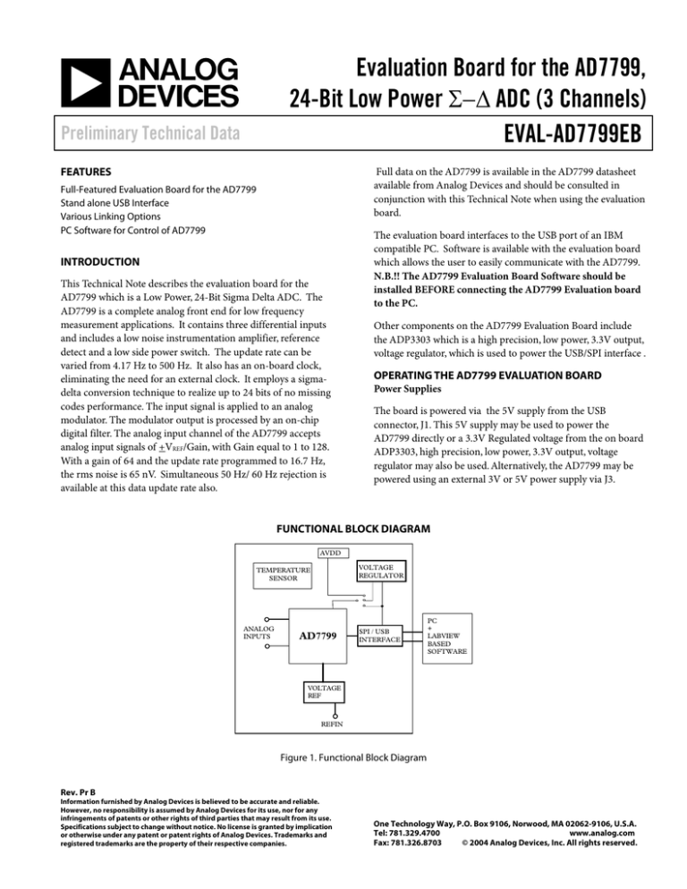
FUNCTIONAL BLOCK DIAGRAM
AVDD
VOLTAGE
REGULATOR
TEMPERATURE
SENSOR
ANALOG
INPUTS
AD7799
SPI / USB
INTERFACE
PC
+
LABVIEW
BASED
SOFTWARE
VOLTAGE
REF
REFIN
Figure 1. Functional Block Diagram
Rev. Pr B
Information furnished by Analog Devices is believed to be accurate and reliable.
However, no responsibility is assumed by Analog Devices for its use, nor for any
infringements of patents or other rights of third parties that may result from its use.
Specifications subject to change without notice. No license is granted by implication
or otherwise under any patent or patent rights of Analog Devices. Trademarks and
registered trademarks are the property of their respective companies.
One Technology Way, P.O. Box 9106, Norwood, MA 02062-9106, U.S.A.
www.analog.com
Tel: 781.329.4700
Fax: 781.326.8703
© 2004 Analog Devices, Inc. All rights reserved.
EVAL-AD7799EB
Preliminary Technical Data
There are ten link options which must be set for the required operating setup before using the evaluation board. The functions of these
link options are outlined below.
Table 1.Evaluation Board Link Settings
Link
LK1, LK2
Default
In
LK3, LK4, LK5, LK6
Out
Description
These links are used to connect the AIN1(+) and AIN1(-) inputs to a reference voltage which
equals AVDD /2. With this configuration, a noise analysis can be performed. With these links
removed, an external voltage may be applied to AIN1 using the SMB connectors.
These links are used to connect the on board temperature demonstration circuit to the ADC,
and must all be in place when attempting to measure ambient temperature.
When LK3 and LK4 are inserted, the 1KΩ thermistor is connected to AIN2. With LK5 and
LK6 in place, a 5KΩ precision resistor is used to generate the reference. This results in a
ratiometric configuration.
LK7, LK8
In
A resistor divider network generates a voltage equal to AVDD /2 which can be used as the
reference for the AD7799. With LK7 and LK8 in place, AVDD /2 is connected to REFIN(+) and
REFIN(-) is connected to GND. To use another reference source, remove LK7 and LK8.
LK9
B
LK9 is used to select the power source for AVDD on the AD7799. LK9 in position A selects an
external power supply, supplied via J3. LK9 in position B selects the 3.3V regulated output from
the onboard ADP3303 voltage regulator. LK9 in position C selects the 5V supply from the USB
connector, J1.
LK10
In
LK10 is used to test the on chip low side power switch. With LK10 in place, enabling the lowside power switch in software by setting a bit in the configuration register turns on the LED, D2
Clearing this bit turns off the LED.
SET-UP CONDITIONS
Care should be taken before applying power and signals to the evaluation board to ensure that all link positions are as per the required
operating mode. Table 1 shows the position in which all the links are set when the evaluation board is sent out.
Table 2: Initial Link and Switch Positions
Link No.
Position
Function
LK1 - LK2
In
AIN1(+) and AIN1(-) are shorted to the reference voltage
LK3 – LK6
Out
The demonstration circuit is disconnected from the AD7799
LK7 – LK8
In
The reference voltage is set to 1.65V (3.3V/2)
LK9
B
The 3.3V supply is used as AVDD for the AD7799.
LK10
In
LED D2 is connected to the Low Side Power Switch of the
AD7799
EVALUATION BOARD INTERFACING
Interfacing to the evaluation board is via a standard USB Connector, J1. J1 is used to connect the evaluation board to the USB port of a
PC. A standard USB connector cable is included with the AD7799 evaluation board to allow the evaluation board to interface with the
PC's USB port. As the board is powered via the USB connector, there is no need for an external power supply, although one may be
connected if preferred via J3.
Communication between the AD7799 and the PC is over the USB/SPI interface. The onboard USB controller (U2) controls this
communication. Remember, the AD7799 Evaluation Board Software should be installed (using the supplied AD7799 Evaluation Board
CD ROM) BEFORE connecting the board to the PC.
Rev. Pr B| Page 2
Preliminary Technical Data
EVAL-AD7799EB
After the AD7799 Evaluation Board Software has been installed, connect the board to the PC via J1 on the AD7799 Evaluation Board
and the USB port on the PC using the supplied USB connector cable. The PC will automatically find the new USB device and will identify
it as: AD7799 Evaluation Board. Follow the onscreen instructions that appear automatically. During the installation process if the
following window appears:
.
Hit Continue Anyway in order to successfully complete the installation of the AD7799 Evaluation Board.
SOCKETS
There are five sockets relevant to the operation of the AD7799 on this evaluation board. The functions of these sockets are outlined in
Table 3.
Table 3. Socket Functions
Socket
Function
AIN1+
Sub-Miniature BNC (SMB) Connector. The analog input signal for the AIN1(+) input of the AD7799 is
applied to this socket.
AIN1-
Sub-Miniature BNC (SMB) Connector. The analog input signal for the AIN1(-) input of the AD7799 is
applied to this socket.
REFIN+
Sub-Miniature BNC (SMB) Connector. This socket is used in conjunction with REFIN(-) to apply an
external reference to the AD7799. The voltage for the REFIN(+) input of the AD7799 is applied to this
socket.
REFIN-
Sub-Miniature BNC (SMB) Connector. This socket is used in conjunction with REFIN(+) to apply an
external reference to the AD7799.The voltage for the REFIN(-) input of the AD7799 is applied to this
socket.
J2
34 Pin (2x16) pin Straight Header. This Socket is used in conjunction with the prototype area to interface
any signal to the AD7799. It is specifically designed as a socket for a 34 pin header.
Rev. Pr B | Page 3


