Construction of Microcontroller Based Digital Voltmeter
advertisement
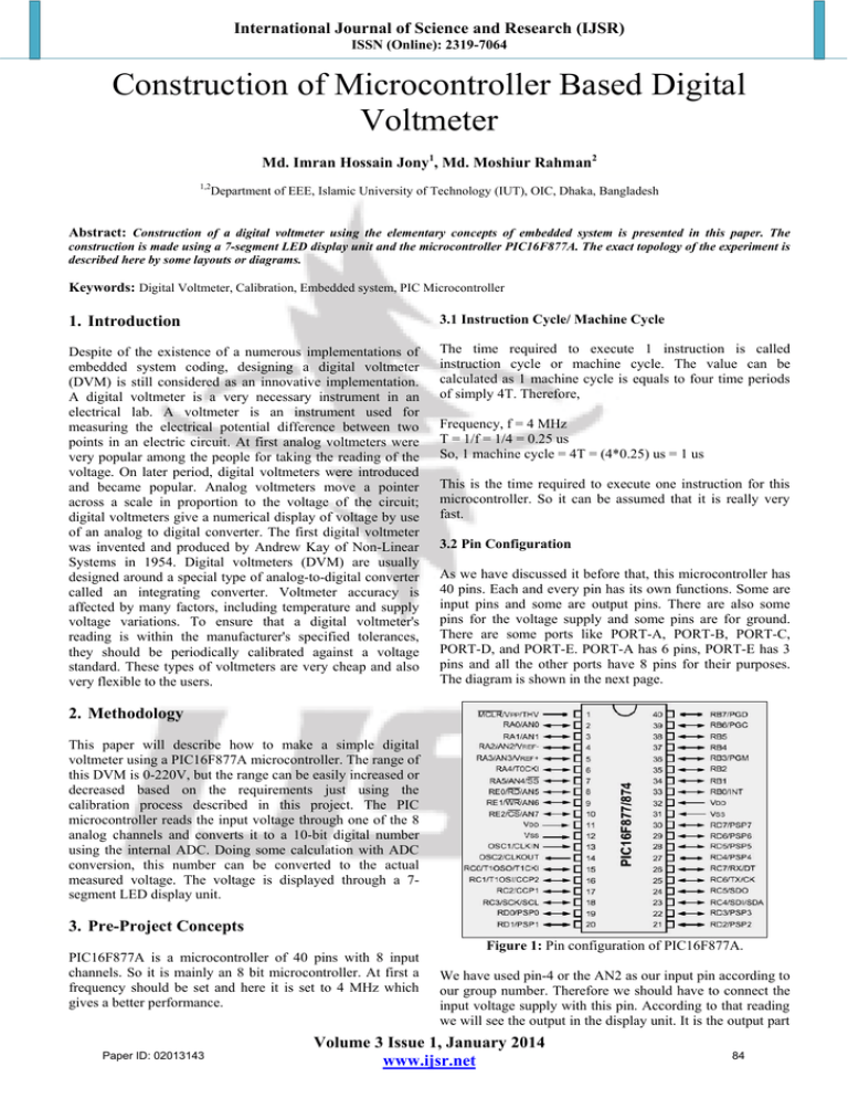
International Journal of Science and Research (IJSR) ISSN (Online): 2319-7064 Construction of Microcontroller Based Digital Voltmeter Md. Imran Hossain Jony1, Md. Moshiur Rahman2 1,2 Department of EEE, Islamic University of Technology (IUT), OIC, Dhaka, Bangladesh Abstract: Construction of a digital voltmeter using the elementary concepts of embedded system is presented in this paper. The construction is made using a 7-segment LED display unit and the microcontroller PIC16F877A. The exact topology of the experiment is described here by some layouts or diagrams. Keywords: Digital Voltmeter, Calibration, Embedded system, PIC Microcontroller 1. Introduction 3.1 Instruction Cycle/ Machine Cycle Despite of the existence of a numerous implementations of embedded system coding, designing a digital voltmeter (DVM) is still considered as an innovative implementation. A digital voltmeter is a very necessary instrument in an electrical lab. A voltmeter is an instrument used for measuring the electrical potential difference between two points in an electric circuit. At first analog voltmeters were very popular among the people for taking the reading of the voltage. On later period, digital voltmeters were introduced and became popular. Analog voltmeters move a pointer across a scale in proportion to the voltage of the circuit; digital voltmeters give a numerical display of voltage by use of an analog to digital converter. The first digital voltmeter was invented and produced by Andrew Kay of Non-Linear Systems in 1954. Digital voltmeters (DVM) are usually designed around a special type of analog-to-digital converter called an integrating converter. Voltmeter accuracy is affected by many factors, including temperature and supply voltage variations. To ensure that a digital voltmeter's reading is within the manufacturer's specified tolerances, they should be periodically calibrated against a voltage standard. These types of voltmeters are very cheap and also very flexible to the users. The time required to execute 1 instruction is called instruction cycle or machine cycle. The value can be calculated as 1 machine cycle is equals to four time periods of simply 4T. Therefore, Frequency, f = 4 MHz T = 1/f = 1/4 = 0.25 us So, 1 machine cycle = 4T = (4*0.25) us = 1 us This is the time required to execute one instruction for this microcontroller. So it can be assumed that it is really very fast. 3.2 Pin Configuration As we have discussed it before that, this microcontroller has 40 pins. Each and every pin has its own functions. Some are input pins and some are output pins. There are also some pins for the voltage supply and some pins are for ground. There are some ports like PORT-A, PORT-B, PORT-C, PORT-D, and PORT-E. PORT-A has 6 pins, PORT-E has 3 pins and all the other ports have 8 pins for their purposes. The diagram is shown in the next page. 2. Methodology This paper will describe how to make a simple digital voltmeter using a PIC16F877A microcontroller. The range of this DVM is 0-220V, but the range can be easily increased or decreased based on the requirements just using the calibration process described in this project. The PIC microcontroller reads the input voltage through one of the 8 analog channels and converts it to a 10-bit digital number using the internal ADC. Doing some calculation with ADC conversion, this number can be converted to the actual measured voltage. The voltage is displayed through a 7segment LED display unit. 3. Pre-Project Concepts PIC16F877A is a microcontroller of 40 pins with 8 input channels. So it is mainly an 8 bit microcontroller. At first a frequency should be set and here it is set to 4 MHz which gives a better performance. Paper ID: 02013143 Figure 1: Pin configuration of PIC16F877A. We have used pin-4 or the AN2 as our input pin according to our group number. Therefore we should have to connect the input voltage supply with this pin. According to that reading we will see the output in the display unit. It is the output part Volume 3 Issue 1, January 2014 www.ijsr.net 84 International Journal of Science and Research (IJSR) ISSN (Online): 2319-7064 of the microcontroller. At inside there are lots of general and special purpose registers. Those which are user defined registers are called the general purpose registers, like c1, c2, d1, d2 etc. Some special purpose registers are: STATUS register, OPTION_REG register, INTCON registers, TMR0 register, ADCON0 register, ADCON1 register, ADRESH and ADRESL registers etc. 3.3 Analog to Digital Converter Module Figure 2: 7-Segment display The Analog-to-Digital (A/D) Converter module has five inputs for the 28-pin devices and eight for the 40/44-pin devices. The conversion of an analog input signal results in a corresponding 10-bit digital number. The A/D module has high and low-voltage reference input that is software selectable to some combination of VDD, VSS, RA2 or RA3. The A/D converter has a unique feature of being able to operate while the device is in Sleep mode. To operate in Sleep, the A/D clock must be derived from the A/D’s internal RC oscillator. The A/D module has four registers. Table 1: Showing different digits. Digits Decimal value 0 126 1 48 2 109 3 121 4 51 5 91 6 95 7 112 8 127 9 123 These registers are: • A/D Result High Register (ADRESH) • A/D Result Low Register (ADRESL) • A/D Control Register 0 (ADCON0) • A/D Control Register 1 (ADCON1) 4. Project Analysis The ADCON0 register controls the operation of the A/D module. The first bit of it is ADON. If we set it to 1, then the conversion starts. We can select the analog channels by changing the configuration of CHS2:CHS0 bits. We have selected ‘010’ for selecting AN2. The ADCON1 register configures the functions of the port pins. The port pins can be configured as analog inputs (RA3 can also be the voltage reference) or as digital I/O. the last bit of ADCON1 is called the ADFM bit. If we set it to 1, then right justification occurred. But we will use the left justification. That’s why we will set it to 0; therefore ADRESH will contain the highest bits. So we will send the value of ADRESH to our desired port to display the value. 4.1 Components Used The ADRESH, ADRESL registers contain the 10-bit result of the A/D conversion. When the A/D conversion is complete, the result is loaded into this A/D Result register pair, the GO/DONE bit (ADCON0<2>) is cleared and the A/D interrupt flag bit ADIF is set. The block diagram of the A/D module is shown in Figure 11-1. After the A/D module has been configured as desired, the selected channel must be acquired before the conversion is started. The analog input channels must have their corresponding TRIS bits selected as inputs [3]. a 1 0 1 1 0 1 1 1 1 1 b 1 1 1 1 1 0 0 1 1 1 c 1 1 0 1 1 1 1 1 1 1 d 1 0 1 1 0 1 1 0 1 1 e 1 0 1 0 0 0 1 0 1 0 f 1 0 0 0 1 1 1 0 1 1 g 0 0 1 1 1 1 1 0 1 1 The project is divided into two parts- software part and the hardware part. Software part is dealt with nothing but the code. In the hardware part a great bit of work is done as because a voltage sensor is not available in our traditional electrical market. Though it is not very tough to construct a voltage sensor, but the important thing is that it needs to be constructed to rectify the voltage. 1. 2. 3. 4. 5. 6. 7. 8. Transformer (12*2) PIC16F877A Capacitor (1 uf) Diodes Resistors (10K) Variable resistor AC cord Connecting wires 4.2 Calibration Calibration is a comparison between measurements – one of known magnitude or correctness made or set with one device and another measurement made in as similar a way as possible with a second device. Calibration means to calibrate or adjust between two different values of voltage to get the desired output. 3.4 Working Principle of 7-Segment Led Display In order to turn on the lights to show the desired digits it is important to understand the working principle of 7-segment LED display unit [1]. Figure 3: Calibration circuit Paper ID: 02013143 Volume 3 Issue 1, January 2014 www.ijsr.net 85 International Journal of Science and Research (IJSR) ISSN (Online): 2319-7064 Here the transformer transforms the 220 V to 12 V first as it is a 12*2 transformer [4]. Two diodes are used to make the AC voltage to DC by rectifying it through full-wave rectification. Then to stabilize the voltage a capacitor is used. To grab the voltage a resistor is put just in parallel to the capacitor. Therefore 12 V will be shown across the resistor. Again two resistors (series) are connected just parallel to the previous resistor. Between these two, one was variable resistor. It should be varied with respect to the display part. While adjusting it with 220 V the experiment is then stopped. This is called the calibration. It has to be done as because the Microchip can operate within the analog signal from 0-5 V. So it can be said that the maximum input voltage of 220V is calibrated as 5V to the chip. 4.3 Full-Wave Rectification the value of ADRESH is sent to PORT-B in order to display the value. Channel 2 of the microcontroller is used here. So the input will be given at PIN-4 of the microcontroller. Mainly the PORT-A was used as the analog input port and PORT-B as output. That’s why binary value of ‘11111111’ is sent to TRISA to make all the pins of PORT-A as input pins. Vice-versa was done for PORT-B. That’s how the process is done. The code is then compiled using a compiler which converts the language to assembly language to make it readable for the microcontroller. 4.5 Results This snap is taken when the voltage was adjusted just at 220V. Therefore the project is successful. Now the voltmeter is ready to measure any voltage ranges from 0-220V. Full wave rectification is done by the two diodes. The output is got both for positive and negative half cycle of the input voltage [2]. Figure 6: Digital voltmeter with 7-segment display (in the lab). 5. Conclusion Figure 4: Full wave rectification. 4.4 Software Portion Code is written in the MPLAB software. The code is mainly based on the concept of binary to BCD conversion. This process is described through a flow chart given below. This project successfully executed a relatively cheaper voltmeter, comparing to those present in the market. This research will enhance the possibility of using digital voltmeters to improve small industries in Bangladesh. Reference [1] Ronald J. Tocci, Neal S. Widmer, Gregory L. Moss Digital Systems, principles and applications. [2] Muhammad H. Rashid - Power Electronics circuits, devices and applications. [3] Data sheet of PIC16F877A. [4] Bhag S. Guru, Huseyin R. Hiziroglu - Electric Machinery And Transformers. Author Profile Figure 5: Flow chart of the code. Md. Imran Hossain Jony: Md. Imran Hossain Jony is a lecturer in the Department of Electrical and Electronic Engineering at City University (CU), Bangladesh. Prior to joining the City University he served as an intern at Energypac Engineering Ltd. for about 3 months in the year of 2012. He has obtained his B.Sc degree in Electrical and Electronic Engineering from Independent University, Bangladesh (IUB) in the same year. Now he also continues his M.Sc study in Electrical and Electronic Engineering at Islamic University of Technology (IUT), OIC, Dhaka, Bangladesh. His research interests are Digital & Wireless Communication. The delay used in this code is 0.125 sec. Left justification is done to get the higher bits in ADRESH resistor. Therefore Paper ID: 02013143 Volume 3 Issue 1, January 2014 www.ijsr.net 86 International Journal of Science and Research (IJSR) ISSN (Online): 2319-7064 Md. Moshiur Rahman: Md Moshiur Rahman obtained his B.Sc degree in electrical and electronic engineering with Honors from University of Asia Pacific (UAP) in 2011. After completed his bachelor degree he joined as a full time faculty (Lecturer) at University of Asia Pacific in the year 2011, also he continued his M.Sc study in electrical and electronic engineering at Islamic University of Technology (IUT), OIC, Dhaka, Bangladesh. His research interests are Digital Electronics, Measurements & Instrumentation and VLSI technology. Paper ID: 02013143 Volume 3 Issue 1, January 2014 www.ijsr.net 87


