AMMP-6222
7 to 21 GHz GaAs High Linearity LNA in SMT Package
Data Sheet
Description
Features
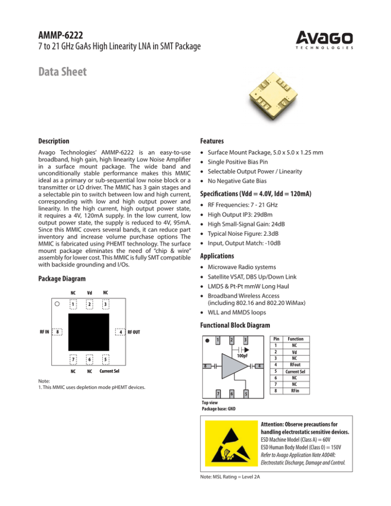
Avago Technologies’ AMMP-6222 is an easy-to-use
broadband, high gain, high linearity Low Noise Amplifier
in a surface mount package. The wide band and
unconditionally stable performance makes this MMIC
ideal as a primary or sub-sequential low noise block or a
transmitter or LO driver. The MMIC has 3 gain stages and
a selectable pin to switch between low and high current,
corresponding with low and high output power and
linearity. In the high current, high output power state,
it requires a 4V, 120mA supply. In the low current, low
output power state, the supply is reduced to 4V, 95mA.
Since this MMIC covers several bands, it can reduce part
inventory and increase volume purchase options The
MMIC is fabricated using PHEMT technology. The surface
mount package eliminates the need of “chip & wire”
assembly for lower cost. This MMIC is fully SMT compatible
with backside grounding and I/Os.
•
•
•
•
Package Diagram
RF IN
NC
Vd
NC
1
2
3
8
4
RF OUT
Surface Mount Package, 5.0 x 5.0 x 1.25 mm
Single Positive Bias Pin
Selectable Output Power / Linearity
No Negative Gate Bias
Specifications (Vdd = 4.0V, Idd = 120mA)
•
•
•
•
•
RF Frequencies: 7 - 21 GHz
High Output IP3: 29dBm
High Small-Signal Gain: 24dB
Typical Noise Figure: 2.3dB
Input, Output Match: -10dB
Applications
•
•
•
•
Microwave Radio systems
Satellite VSAT, DBS Up/Down Link
LMDS & Pt-Pt mmW Long Haul
Broadband Wireless Access
(including 802.16 and 802.20 WiMax)
• WLL and MMDS loops
Functional Block Diagram
1
7
6
NC
NC
2
100pF
5
Current Sel
3
8
4
Note:
1. This MMIC uses depletion mode pHEMT devices.
7
6
5
Pin
1
2
3
4
5
6
7
8
Function
NC
Vd
NC
RFout
Current Sel
NC
NC
RFin
Top view
Package base: GND
Attention: Observe precautions for
handling electrostatic sensitive devices.
ESD Machine Model (Class A) = 60V
ESD Human Body Model (Class 0) = 150V
Refer to Avago Application Note A004R:
Electrostatic Discharge, Damage and Control.
Note: MSL Rating = Level 2A
Electrical Specifications
1. Small/Large -signal data measured in a fully de-embedded test fixture form TA = 25°C.
2. Pre-assembly into package performance verified 100% on-wafer per AMMC-6222 published specifications.
3. This final package part performance is verified by a functional test correlated to actual performance at one or more
frequencies.
4. Specifications are derived from measurements in a 50 Ω test environment. Aspects of the amplifier performance may
be improved over a more narrow bandwidth by application of additional conjugate, linearity, or low noise (Гopt)
matching.
5. All tested parameters guaranteed with measurement accuracy +/-0.5dB for gain and +/-0.3dB for NF in the high
output power configuration.
Table 1. RF Electrical Characteristics
TA=25°C, Id=120mA, Vd=4.0V, Zo=50 Ω
High Output Power Configuration
Parameter
Min
Typical
Drain Current, Id
Small Signal Gain, Gain
Lower Output Power Configuration
Max
Min
Typical
Max
Unit
Comment
120
95
mA
24
23
dB
Test frequency =
8, 14, 18 GHz
2.3
dB
Test frequency =
8, 14, 18 GHz
19
Noise Figure into 50 Ω, NF
2.3
3.5
Output Power at 1dB
Gain Compression, P1dB
15.5
14
dBm
Output Power at 3dB
Gain Compression, P3dB
17.5
16
dBm
Output Third Order
Intercept Point, OIP3
29
27
dBm
Isolation, Iso
-45
-45
dB
Input Return Loss, Rlin
-10
-10
dB
Output Return Loss, RLout
-10
-10
dB
Table 2. Recommended Operating Range
1. Ambient operational temperature TA = 25°C unless otherwise noted.
2. Channel-to-backside Thermal Resistance (Tchannel (Tc) = 34°C) as measured using infrared microscopy. Thermal
Resistance at backside temperature (Tb) = 25°C calculated from measured data.
Description
Min.
Typical
Max.
Unit
Comments
Drain Supply Current, Id
80
120
160
mA
Vd = 4.5 V, Under any RF power drive and temperature
Drain Supply Voltage, Vd
3
4
5
V
2
Table 3. Thermal Properties
Parameter
Test Conditions
Value
Thermal Resistance, qjc
Ambient operational temperature TA = 25°C
Channel-to-backside Thermal Resistance Tchannel(Tc)=34°C
Thermal Resistance at backside temperature Tb=25°C
qjc = 31.47 °C/W
Absolute Minimum and Maximum Ratings
Table 4. Minimum and Maximum Ratings
Description
Max.
Unit
Drain to Ground Supply Voltage, Vd
5.5
V
Drain Current, Id
170
mA
RF CW Input Power, Pin
10
dBm
Channel Temperature, Tch
+150
°C
+150
°C
260
°C
Storage Temperature, Tstg
Maximum Assembly Temperature, Tmax
Min.
-65
Comments
CW
20 second maximum
Notes: 1. Operation in excess of any one of these conditions may result in permanent damage to this device.
3
AMMP-6222 Typical Performance for High Current, High Output Power Configuration [1], [2]
(TA = 25°C, Vdd=4V, Idd=120mA, Zin = Zout = 50 W unless noted)
30
Noise Fi gure (dB)
5
S 21 (d B)
25
20
15
10
4
3
2
1
0
5
5
10
15
20
6
25
8
10 12 14 16 18 20 22
Fre que nc y (GHz)
Freque nc y (GHz)
Figure 1a. Small-signal Gain
Figure 2a. Noise Figure
0
20
OP 1dB (dBm)
S 11 (d B)
-5
-10
-15
-20
15
10
5
0
-25
5
10
15
20
25
6
8
Freque nc y (GHz)
Figure 4a. Output P-1dB
0
35
-5
30
OIP 3 (dBm)
S22 (dB)
Figure 3a. Input Return Loss
-10
-15
-20
5
10
15
20
Freque nc y (GHz)
Figure 5a. Output Return Loss
10 12 14 16 18 20 22
Frequenc y (GHz)
25
25
20
15
10
6
8
10 12 14 16 18 20 22
Freque nc y (GHz)
Figure 6a. Output IP3
Note:
1. S-parameters are measured with R&D Eval Board as shown in Figure 21. Board and connector effects are included in the data.
2. Noise Figure is measured with R&D Eval board as shown in Figure 21, and with a 3-dB pad at input. Board and connector losses are already deembeded from the data.
4
AMMP-6222 Typical Performance for High Current, High Output Power Configuration (Cont)
-20
150
-30
130
Idd (mA)
S 12 (dB)
(TA = 25°C, Vdd=4V, Idd=120mA, Zin = Zout = 50 W unless noted)
-40
-50
110
-60
5
10
15
20
90
70
25
3
Frequenc y (GHz)
Figure 7a. Isolation
4
Vdd (V)
4.5
5
Figure 8a. Idd over Vdd
30
5
Noise F igure (d B)
25
S 21 (dB)
3.5
20
15
4V
5V
10
3V
4
3
2
3V
1
4V
5V
0
5
5
10
15
20
Freque nc y (GHz)
6
25
8
10
12
14
16
18
20
22
Freque nc y (GHz)
Figure 10a. Noise Figure Over Vdd
Figure 9a. Small-signal Gain Over Vdd
0
0
-10
-20
S2 2 (dB )
S1 1 (dB)
-5
4V
3V
5V
-30
5
10
15
20
Freque nc y (GHz)
Figure 11a. Input Return Loss Over Vdd
5
-10
-15
4V
-20
5V
3V
-25
25
5
10
15
20
Freque ncy (GHz)
Figure 12a. Output Return Loss Over Vdd
25
AMMP-6222 Typical Performance for High Current, High Output Power Configuration (Cont) (TA = 25°C, Vdd=4V, Idd=120mA, Zin = Zout = 50 W unless noted)
20
OIP 3 (dBm)
OP 1dB ( dBm)
25
15
10
3V
5
4V
5V
0
6
8
10
12
14
16
18
20
35
30
25
20
15
10
5
0
3V
4V
5V
6
22
8
Freque nc y (GHz)
Figure 14a. Output IP3 over Vdd
35
Noise F igure (dB)
8
30
S21 (dB)
18 20 22
Freque nc y (GHz)
Figure 13a. Output P1dB over Vdd
25
20
25C
15
85C
10
-40C
5
10
15
20
Fre que ncy (GHz)
-40C
6
25C
85C
4
2
0
5
6
25
8
10 12 14 16 18 20 22
Freque nc y (GHz)
Figure 15a. Small-signal Gain Over Temp
Figure 16a. Noise Figure Over Temp
0
0
25C
-5
-5
-10
-15
S2 2 (dB)
S11 (dB)
10 12 14 16
25C
-40C
-10
-15
-40C
-20
85C
85C
-25
-20
5
10
15
20
Freque ncy (GHz)
Figure 17a. Input Return Loss Over Temp
6
25
5
10
15
20
Freque nc y (GHz)
Figure 18a. Output Return Loss Over Temp
25
AMMP-6222 Typical Performance for Low Current, Low Output Power Configuration [1], [2]
(TA = 25°C, Vdd=4V, Idd=95mA, Zin = Zout = 50 W unless noted)
30
Noise Fi gure (dB)
5
S21 (dB)
25
20
15
10
5
4
3
2
1
0
5
10
15
20
25
6
8
10 12 14 16 18 20 22
Freque ncy (GHz)
Freque nc y (GHz)
Figure 1b. Small-signal Gain
Figure 2b. Noise Figure
0
20
OP 1dB (dB m)
S 11 (dB)
-5
-10
-15
-20
-25
5
10
15
20
15
10
5
0
25
6
8
10 12 14 16
Freque ncy (GHz)
Figure 3b. Input Return Loss
Figure 4b. Output P-1dB
0
35
-5
OIP3 (dBm)
S 22 (dB )
18 20 22
Freque nc y (GHz)
-10
-15
30
25
20
15
10
-20
5
10
15
20
25
6
8
Freque nc y ( GHz)
Freque nc y (GHz)
Figure 5b. Output Return Loss
10 12 14 16 18 20 22
Figure 6b. Output IP3
Note:
1. S-parameters are measured with R&D Eval Board as shown in Figure 21. Board and connector effects are included in the data.
2. Noise Figure is measured with R&D Eval board as shown in Figure 21, and with a 3-dB pad at input. Board and connector losses are already deembeded from the data
7
AMMP-6222 Typical Performance for Low Current, Low Output Power Configuration (Cont)
-20
130
-30
110
Idd (mA)
S1 2 (dB)
(TA = 25°C, Vdd=4V, Idd=95mA, Zin = Zout = 50 W unless noted)
-40
90
-50
70
-60
50
5
10
15
20
3
25
3.5
Freque nc y (GHz)
Figure 7b. Isolation
Noise Fi gure (dB)
S 21 (d B)
5
5
25
20
15
4V
5V
10
3V
5
10
15
20
Freque nc y (GHz)
4
3
2
3V
1
4V
5V
0
5
6
25
-5
-5
-10
-10
S 22 (dB )
0
-15
4V
3V
-25
-30
10
15
20
Freque nc y (GHz)
Figure 11b. Input Return Loss Over Vdd
12
14
16
18
20
22
-15
4V
-20
5V
-25
5V
5
10
Figure 10b. Noise Figure Over Vdd
0
-20
8
Freque nc y (GHz)
Figure 9b. Small-signal Gain Over Vdd
S 11 (d B)
4.5
Figure 8b. Idd over Vdd
30
8
4
Vdd (V)
25
3V
-30
5
10
15
20
Freque nc y (GHz)
Figure 12b. Output Return Loss Over Vdd
25
AMMP-6222 Typical Performance for Low Current, Low Output Power Configuration (Cont)
(TA = 25°C, Vdd=4V, Idd=95mA, Zin = Zout = 50 W unless noted)
15
OI P 3 (dB m )
OP1dB ( dBm )
20
10
3V
5
4V
5V
0
6
8
10
12
14
16
18
20
35
30
25
20
15
10
5
0
3V
4V
5V
6
22
8
Freque nc y (GHz)
Freque nc y (GHz)
Figure 13b. Output P1dB over Vdd
Figure 14b. Output IP3 over Vdd
35
8
Nois e Fi gure (dB)
S21 (dB)
30
25
20
25C
15
85C
10
-40C
5
5
10
15
20
Fre que nc y (GHz)
25C
85C
4
2
6
25
0
-5
-5
-10
-10
-15
25C
-40C
-25
10 12 14 16 18 20 22
Figure 16b. Noise Figure Over Temp
0
-20
8
Freque nc y (GHz)
S22 (dB)
S11 (dB)
-40C
6
0
Figure 15b. Small-signal Gain Over Temp
-15
25C
-20
85C
-25
85C
-30
-40C
-30
5
10
15
20
Freque nc y (GHz)
Figure 17b. Input Return Loss Over Temp
9
10 12 14 16 18 20 22
25
5
10
15
20
Frequenc y (GHz)
Figure 18b. Output Return Loss Over Temp
25
AMMP-6222 Application and Usage
Biasing and Operation
4V
Vdd
1
IN
0.1uF
2
3
100pF
8
4
7
The AMMP-6222 is normally biased with a positive
drain supply connected to the VDD pin through
bypass capacitor as shown in Figures 19 and 20. The
recommended drain supply voltage for general usage is
4V and the corresponding drain current is approximately
120mA. It is important to have 0.1uF bypass capacitor and
the capacitor should be placed as close to the component
as possible. Aspects of the amplifier performance may
be improved over a narrower bandwidth by application
of additional conjugate, linearity, or low noise (Topt)
matching.
6
OUT
5
For receiver front end low noise applications where high
power and linearity are not often required, the AMMP6222 can be set in low current state when pin # 5 is open
as shown in Figure 19. In this configuration, the bias
current is approximately 90mA, 95mA and 100mA for 3V,
4V and 5V respectively.
Open
Figure 19. Low Current, Low Output Power State
4V
Vdd
1
IN
0.1uF
2
100pF
8
4
7
6
In applications where high output power and linearity
are often required such as LO or transmitter drivers, the
AMMP-6222 can be selected to operate at its highest
output power by grounding pin # 5 as shown in Figure 20.
At 5V, the amplifier can provide Psat of ~ 20dBm. The bias
current in this configuration is 115mA, 120mA and 125mA
for 3V, 4V and 5V respectively.
3
OUT
5
Refer the Absolute Maximum Ratings table for allowed DC
and thermal conditions.
Figure 20. High Current, High Output Power State
Figure 21. Evaluation/Test Board (available to qualified customer request)
Vd2
Vd1
In
Matching
Network
Out
Matching
Network
SELECT
Figure 22. Simplified High Linearity LNA Schematic
10
Typical Scattering Parameters
Please refer to <http://www.avagotech.com> for typical scattering parameters data.
Package Dimension, PCB Layout and Tape and Reel information
Please refer to Avago Technologies Application Note 5520, AMxP-xxxx production Assembly Process (Land Pattern A).
Ordering Information
Devices Per
Container
Container
AMMP-6222-BLKG
10
Antistatic bag
AMMP-6222-TR1G
100
7” Reel
AMMP-6222-TR2G
500
7” Reel
Part Number
For product information and a complete list of distributors, please go to our web site:
www.avagotech.com
Avago, Avago Technologies, and the A logo are trademarks of Avago Technologies in the United States and other countries.
Data subject to change. Copyright © 2005-2013 Avago Technologies. All rights reserved. Obsoletes AV01-0441EN
AV02-0493EN - July 8, 2013
