ISSN 2322-0929
Vol.04, Issue.01,
January-2016,
Pages:0012-0016
www.ijvdcs.org
A Low Power VDD Moduled SRAM Cell With Sense Amplifier
P. GOWRI SWETHA1, T. UMA MAHESWARI2
1
PG Scholar, Dept of ECE(VLSI & ES), Vignan Institute of Engineering For Women‟s for Woman‟s, Visakhapatnam, AP, India.
2
Assistant Professor, Dept of ECE, Vignan Institute of Engineering For Women‟s for Woman‟s, Visakhapatnam, AP, India.
Abstract: Ultra Dynamic Voltage Scaling (UDVS) and Transient Negative Bit Line Voltage (NBLV) techniques are used in this
paper, for reducing the power consumption as well as reducing delays while in the all operating modes of 6T SRAM cell.
Scaling voltages using UDVS technique can reduce the leakage powers and delays. In different modes of cell operation, UDVS
technique scales the supply voltage and gives scalable voltage to different circuits. As per the requirement, scalable voltage gives
to writer circuit or SRAM cell during the write operation. In this paper introduce Transient Negative Bit Line Technique
(TNBL), It is a write assist scheme. By using this scheme performs write operation fastly and it performs write operation without
using any on chip or off chip voltage source. Read assist circuits are also developed for better read performance. Using this read
assist circuits to basic SRAM cell for reading the data from the cell without changing any cell data. In this paper finally
developed 6T SRAM cell with low power consumption and less delay with 90nm technology in TANNER TOOL.
Keywords: Tran-NBL, NBLV, U-DVS.
I. INTRODUCTION
Now a day‟s designing any circuit or a system power
reduction is very important, at the same time performance
also takes on consideration. Static Random Access Memory
(SRAM) is a volatile memory. Designing any Die in the
research area, SRAM cells occupies more than 50% of area
on Die. So, reduce the SRAM cell power consumption in
write and read operations then easily reduce the power
consumption to a particular circuit or a system. Power
saving is an important consideration in designing SRAM
cells. For reducing the power consumption used by
Transient Negative Bit Line technique (TNBL). This TNBL
technique is a best choice for reducing the power
consumption by adjusting the bit line voltages to the SRAM
cell as per the requirement [1]. In this paper introduced
voltage scaling and design issues of SRAM cell basic circuit
diagram and Transient Negative Bit-line Write Assist
Scheme.
II. 6T SRAM CELL
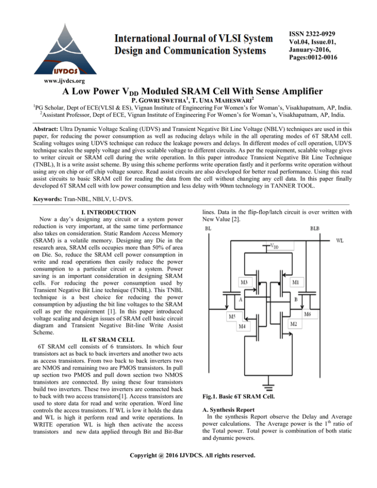
6T SRAM cell consists of 6 transistors. In which four
transistors act as back to back inverters and another two acts
as access transistors. From two back to back inverters two
are NMOS and remaining two are PMOS transistors. In pull
up section two PMOS and pull down section two NMOS
transistors are connected. By using these four transistors
build two inverters. These two inverters are connected back
to back with two access transistors[1]. Access transistors are
used to store data for read and write operation. Word line
controls the access transistors. If WL is low it holds the data
and WL is high it perform read and write operations. In
WRITE operation WL is high then activate the access
transistors and new data applied through Bit and Bit-Bar
lines. Data in the flip-flop/latch circuit is over written with
New Value [2].
Fig.1. Basic 6T SRAM Cell.
A. Synthesis Report
In the synthesis Report observe the Delay and Average
power calculations. The Average power is the 1 th ratio of
the Total power. Total power is combination of both static
and dynamic powers.
Copyright @ 2016 IJVDCS. All rights reserved.
P. GOWRI SWETHA, T. UMA MAHESWARI
UDVS based 6T SRAM cell is a combination of UDVS
circuit, write circuit, SRAM cell and Read circuit.
A. Write Driver Circuit
In order to read the write driver circuit drives the
appropriate data values onto the bit line true and
compliment lines. Since the primary objective data from an
SRAM, the Data must write into memory first as shown in
Fig.5. The four vertical devices in series are often referred
to as a gated inverter. When write enable is asserted high is
to drive a “0”, the NMOS and PMOS may be similarly
sized, rather than the typical two to one ratio.
Fig.2. Observe Delay and Avg.Power Consumption.
B. 6T SRAM Cell Output Waveforms
Fig.5. write driver circuit.
Fig.3. Output for Basic 6T SRAM Cell.
The above three figs.1, 2, 3 showed 6T SRAM cell
working. When VDD and WL is high 6T SRAM cell takes
data from bit, bit-bar, store the value into the cell. Bit, Bitbar values are exact complimented values. Output of the bit
signal is exact compliment of the Bit-Bar signal.
B. Read Circuit
Read circuit is used to read the data from SRAM cell.
Read circuit is combination of pre-charge circuit, isolation
circuit, sense amplifier.
Pre-Charge Circuit:
III. U-DVS BASED 6T SRAM CELL
Fig.6. pre-charge circuit.
Fig.4. U-DVS based 6T SRAM cell Write and Read
operation.
Pre-charge circuit is a three transistor circuit as shown
in fig 6. Out of three, two transistors are used for pre-charge
the bit lines and remaining transistor used for avoid
capacitive coupling between two bit lines. In the pre charge
circuit, below two PMOS transistors drains are connected to
VDD and sources are connected to BIT and BITB. Due to this
connection BIT and BITB are pre charged to VDD and word
line is high then connecting the internal nodes of the bit
International Journal of VLSI System Design and Communication Systems
Volume.04, IssueNo.01, January-2016, Pages: 0012-0016
A Low Power VDD Moduled SRAM Cell With Sense Amplifier
lines. In read operation any one of the bit line discharges via
the node storing „0‟ at the same time other bit line maintains
VDD. So, between two bit lines differential voltage (Vd) is
developed (that means, one bit line voltage remains at V DD
the discharges to (VDD-Vd)).
Isolation Circuit:
Fig.9. Output Wave Form.
Fig.7. isolation circuit.
Isolation circuit is a two transistor circuit. It consists of
two PMOS transistors. Using this two transistors bit lines
are connected to sense amplifier as shown in fig 7.. After
generating the voltage difference between the two bit lines,
isolation circuit isolates the SRAM cell and SENSE
AMPLIFIER. Isolation circuit enabled only after completion
of voltage difference. Due to this reason, increasing the
sense amplifier circuit performance, bit lines are isolated
[4].
Synthesis Report of U-DVS based 6T SRAM cell:
Synthesis Report of U-DVS based 6T SRAM cell as shown
in Fig.10.
Sense Amplifier: Sense amplifiers place a major role in
SRAM cell read operation. It reduces the overall SRAM
chip Delay and Power Consumption. In READ operation
lower voltage swing is occurred. By using the sense
amplifier, can amplify the voltage coming from bit lines as
shown in Fig.8. But the sense amplifier output voltage is
fully swings from 0 to VDD[3].
Fig.10. results for power and delay.
IV. 6T SRAM WRITE WITH TRANSIENT
NEGATIVE BIT LINE AND READ
With the help of Negative Bit Line Technique the write
operation will be easy to perform. Important work is, apply
negative voltage to pass transistor source terminal, when
WL is high. So channel band width is increased due to
negative voltage source and gate voltage. Channel band
width increases between source and drain terminals of the
pass transistor. If channel is more, then data easily write into
the cell[7].
(1)
Here Vgs= Vg-Vs
Apply source voltage is negative
Fig.8. Sense Amplifier.
Out Puts of U-DVS based 6T SRAM Cell: Out Puts of UDVS based 6T SRAM Cell as shown in Fig.9.
International Journal of VLSI System Design and Communication Systems
Volume.04, IssueNo.01, January-2016, Pages: 0012-0016
(2)
P. GOWRI SWETHA, T. UMA MAHESWARI
So Vgs increases, Id increased, then channel increased
B. Mode Changes Voltage To Negative
between the source and drain terminal.
Mode Changes Voltage To Negative as shown in Fig.13.
Fig.13. Observe Change Voltages.
Fig.11. Tran-NBL 6T SRAM write and read.
Fig.11 is 6T SRAM cell write and read circuit using
transient negative bit line scheme. This circuit consists of
write circuit and read circuit. In the write circuit two
capacitors are used for coupling. Two capacitors are
connected in series, one end of capacitor connected to Bit
and BitB, other end is connected to BIT-EN (BE This
capacitive coupling generates negative voltage due to BITEN signal is low, then one end of capacitor is „0‟ but other
end maintain VDD until sometime i.e. discharging time. If
positive terminal is „0‟, then negative terminal is high
because of capacitor is not discharged suddenly. So, at that
time channel of access transistor is more due to WL voltage
and gate to source voltage. If channel is more data easily
pass into the SRAM cell. So, here improve the performance
of write mode SRAM cell. .[6][7]
A. Synthesis Report of Tran-NBV based 6T SRAM Cell
Synthesis Report of Tran-NBV based 6T SRAM Cell as
shown in Fig.12.
.
Fig.12. Delay and Avg. power result.
C. Output Waveform of Tran-NBV 6T SRAM Cell
Write And Read
Output Waveform of Tran-NBV 6T SRAM Cell Write
And Read as shown in Fig.14.
Fig 14. output waveforms of TRAN-NBV 6T SRAM cell
write and read.
V. RESULTS
TABLE I:
VI. CONCLUSION
In this paper we have successfully crated a SRAM cell
using Transient Negative Bit line technique with 90nm
technology in tanner tool and obtained the functionality of
SRAM with Read and Write and calculated the delay and
International Journal of VLSI System Design and Communication Systems
Volume.04, IssueNo.01, January-2016, Pages: 0012-0016
A Low Power VDD Moduled SRAM Cell With Sense Amplifier
power dissipation of 6T- SRAM Cell, UDVS BASED 6T
SRAM cell and Tran-Negative Bit Line based 6T SRAM
cell. As compared to all the results Tran- negative bit line
technique gives best results.
VII. REFERENCES
[1]S.Mukhopadhyay,R.Rao,J.J.kim,C.T.Chuang, ”capacitive
coupling based Transient Negative Bit-line Voltage(TranNBL) scheme for improving Write-ability of SRAM design
in Nanometer Technologies”, IEEE Conference, pg-no:384387.
[2] Srikanth Lade, Pradeep Kumar Urity,” Analysis of 8T
SRAM with Read and Write Assist Schemes (UDVS) In
45nm CMOS Technology”, International Journal of
Science, Engineering and Technology Research (IJSETR),
Volume 3, Issue 12, December 2014, ISSN:2278-7798,pgno: 3271-3276.
[3] Hassan Mustafa, Mohab anis, Mohamed elmasry
“Statistical SRAM read access yield improvement using
Negative capacitance circuit”, IEEE TRANSACTIONS
ON VERY LARGE SCALE INTEGRATION (VLSI)
SYSTEMS, VOL. 21, NO. 1, JANUARY 2013, pg-no
:
92-101.
[4] Anh-tuan Do,zhi-hui kong,kiat-seng and Jeremy yung
shern “Design And Sensitivity Analysis Of a New
Current Mode Sense Amplifier for Low Power SRAM”
IEEE TRANSACTIONS ON VERY LARGE SCALE
INTEGRATION (VLSI) SYSTEMS, VOL. 19, NO. 2,
FEBRUARY 2011, pg-no:196- 204.
[5] Vibhu Sharma, Stefan Cosemans, Maryam Ashoue, Jos
Huisken, Francky Catthoor,”Ultra Low Power Litho
Friendly Local Assist Circuitry For Variability Resilient 8T
SRAM”, 2012 EDAA.
[6] Maisagalla gopal, D.siva sankar Prasad, “8TSRAM cell
design for dynamic and leakage power reduction”2013.
[7] Ali valaee and Asim j.Al-khalili,” SRAM read assist
scheme for high performance low power application”, 2011
IEEE conference, ISOCC 2011, pg-no: 179-182.
[8] Rajpal Sharma, Gaurav Kumar,” Reliability Aware
Negative Bit-Line Voltage Write Assist Scheme for
SRAM”, International Journal of Advanced Research in
Computer Science and Software Engineering, Volume 3,
Issue 8, August 2013 ISSN: 2277 128X.
International Journal of VLSI System Design and Communication Systems
Volume.04, IssueNo.01, January-2016, Pages: 0012-0016


