MMA032AA
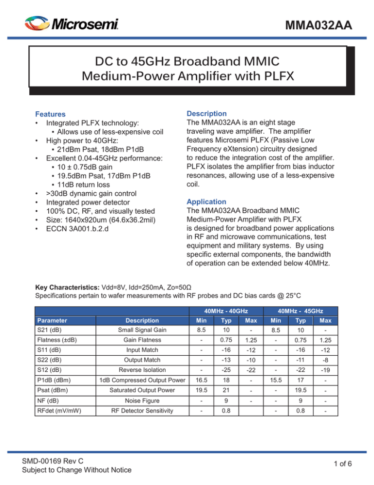
DC to 45GHz Broadband MMIC
Medium-Power Amplifier with PLFX
Features
• Integrated PLFX technology:
▪ Allows use of less-expensive coil
• High power to 40GHz:
▪ 21dBm Psat, 18dBm P1dB
• Excellent 0.04-45GHz performance:
▪ 10 ± 0.75dB gain
▪ 19.5dBm Psat, 17dBm P1dB
▪ 11dB return loss
• >30dB dynamic gain control
• Integrated power detector
• 100% DC, RF, and visually tested
• Size: 1640x920um (64.6x36.2mil)
• ECCN 3A001.b.2.d
Description
The MMA032AA is an eight stage
traveling wave amplifier. The amplifier
features Microsemi PLFX (Passive Low
Frequency eXtension) circuitry designed
to reduce the integration cost of the amplifier.
PLFX isolates the amplifier from bias inductor
resonances, allowing use of a less-expensive
coil.
Application
The MMA032AA Broadband MMIC
Medium-Power Amplifier with PLFX
is designed for broadband power applications
in RF and microwave communications, test
equipment and military systems. By using
specific external components, the bandwidth
of operation can be extended below 40MHz.
Key Characteristics: Vdd=8V, Idd=250mA, Zo=50Ω
Specifications pertain to wafer measurements with RF probes and DC bias cards @ 25°C
40MHz - 40GHz
Parameter
40MHz - 45GHz
Description
Min
Typ
Max
Min
Typ
Max
Small Signal Gain
8.5
10
-
8.5
10
-
Gain Flatness
-
0.75
1.25
-
0.75
1.25
S11 (dB)
Input Match
-
-16
-12
-
-16
-12
S22 (dB)
Output Match
-
-13
-10
-
-11
-8
S12 (dB)
Reverse Isolation
-
-25
-22
-
-22
-19
P1dB (dBm)
1dB Compressed Output Power
16.5
18
-
15.5
17
-
Psat (dBm)
Saturated Output Power
19.5
21
-
-
19.5
-
Noise Figure
-
9
-
-
9
-
RF Detector Sensitivity
-
0.8
-
0.8
-
S21 (dB)
Flatness (±dB)
NF (dB)
RFdet (mV/mW)
SMD-00169 Rev C
Subject to Change Without Notice
1 of 6
MMA032AA
Supplemental Specifications
S21
Noise Figure
Typical IC performance measured on-wafer
Typical IC performance with package de-embedded
S11, S22
S12
Typical IC performance measured on-wafer
Typical IC performance measured on-wafer
Output Power
Group Delay
Typical IC performance measured on-wafer
Typical IC performance measured on-wafer
SMD-00169 Rev C
Subject to Change Without Notice
2 of 6
MMA032AA
Table 1: Supplemental Specifications
Parameter
Description
Min
Typ
Max
Vdd
Drain Bias Voltage
-
8V
8.2V
Idd
Drain Bias Current
-
250mA
300mA
Vg1
1st Gate Bias Voltage
-4V
-
+0.5V
Vg2
2nd Gate Bias Voltage
Vdd - Vg2 < 7V
N/C
+4V
Pin
Input Power (CW)
-
-
23dBm
Pdc
Power Dissipation
-
2W
-
Tch
Channel Temperature
-
-
150˚C
Θch
Thermal Resistance (Tcase=85˚C)
-
21˚ C/W
-
Caution, ESD
Sensitive Device
SMD-00169 Rev C
Subject to Change Without Notice
3 of 6
MMA032AA
DC Bias:
The MMA032AA features a patented on-chip passive bias circuit called ‘PLFX’. This circuit isolates
the amplifier from bias coil resonances above 14GHz, allowing the use of less expensive coils;
traditional biasing requires bias coils with self-resonances outside the operating range of the amplifier.
The device is biased by applying a positive voltage to the drain (Vdd), then setting the drain current
(Idd) using a negative voltage on the gate (Vg1). The nominal bias is Vdd=8V, Idd=250mA.
Improved performance can be achieved with gate bias adjustment; use the drain termination bypass
to alter the output voltage (detected from the drain sense).
Gain Control:
Dynamic gain control is available when operating the amplifier in the linear gain region. Negative
voltage applied to the second gate (Vg2) reduces amplifier gain.
RF Power Detection:
RF output power can be calculated from the difference between the RF detector voltage
and the DC detector voltage, minus a DC offset. Please consult the application note available
on the Microsemi website.
Low-Frequency Use:
The MMA032AA has been designed so that the bandwidth can be extended to low frequencies.
The low end corner frequency of the device is primarily determined by the external biasing
and AC coupling circuitry.
Matching:
The amplifier incorporates on- chip termination resistors on the RF input and output. These
resistors are RF grounded through on-chip capacitors, which are small and become open circuits
at frequencies below 1GHz.
A pair of gate and drain termination bypass pads are provided for connecting external capacitors
required for the low frequency extension network. These capacitors should be 10x the value
of the DC blocking capacitors.
DC Blocks:
The amplifier is DC coupled to the RF input and output pads; DC voltage on these pads must
be isolated from external circuitry.
For operation above 2GHz, a series DC-blocking capacitor with minimum value of 20pF
is recommended; operation down to 40MHz requires a minimum of 120pF.
Bias Inductor:
The patented on-chip LFX circuit eliminates the need for a drain bias choke; the amplifier requires
a bypass capacitor close to the chip and bonded to the drain bias pad. The drain bias supply
is connected directly to the bypass capacitor.
SMD-00169 Rev C
Subject to Change Without Notice
4 of 6
MMA032AA
Die size, pad locations, and pad descriptions
Chip size: 1640x920um (64.6x36.2mil)
Chip size tolerance: ±5um (0.2mil)
Chip thickness: 100 ±10um (4 ±0.4mil)
Pad dimensions: 80x80um (3.1x3.1mil)
Pick-up and Chip Handling:
This MMIC has exposed air bridges on the top surface. Do not pick up chip with vacuum
on the die center; handle from edges or use a collet.
Thermal Heat Sinking:
To avoid damage and for optimum performance, you must observe the maximum channel
temperature and ensure adequate heat sinking.
ESD Handling and Bonding:
This MMIC is ESD sensitive; preventive measures should be taken during handling, die attach,
and bonding.
Epoxy die attach is recommended. Please review our application note MM-APP-0001
handling and die attach recommendations, on our website for more handling, die attach
and bonding information.
SMD-00169 Rev C
Subject to Change Without Notice
5 of 6
MMA032AA
Information contained in this document is proprietary to Microsem. This document may not be modified in any way without the express
written consent of Microsemi. Product processing does not necessarily include testing of all parameters. Microsemi reserves the right to
change the configuration and performance of the product and to discontinue product at any time.
Microsemi Corporate Headquarters
Microsemi Corporation (Nasdaq: MSCC) offers a comprehensive portfolio of semiconductor
One Enterprise, Aliso Viejo CA 92656 USA and system solutions for communications, defense and security, aerospace, and industrial
Within the USA: +1 (949) 380-6100
markets. Products include high-performance and radiation-hardened analog mixed-signal
Sales: +1 (949) 380-6136
integrated circuits, FPGAs, SoCs, and ASICs; power management products; timing and
Fax: +1 (949) 215-4996
synchronization devices and precise time solutions, setting the world’s standard for time;
voice processing devices; RF solutions; discrete components; security technologies and
scalable anti-tamper products; Power-over-Ethernet ICs and midspans; as well as custom
design capabilities and services. Microsemi is headquartered in Aliso Viejo, Calif. and has
approximately 3,400 employees globally. Learn more at www.microsemi.com.
© 2014 Microsemi Corporation. All rights reserved. Microsemi and the Microsemi logo are trademarks of Microsemi Corporation. All other
trademarks and service marks are the property of their respective owners.
SMD-00169 Rev C
Subject to Change Without Notice
6 of 6


