AST-GLSRF
Preliminary
Product Brief
GLONASS RF Downconverter
FEATURES
•
•
•
•
•
•
•
•
•
•
•
•
GENERAL DESCRIPTION
The AST-GLSRF is a high performance, fully
integrated, RF front-end chip for downconversion and
amplification of GLONASS signals. It has been
designed for L1 (1602 MHz),
Single chip GLONASS downconverter
GLONASS L1 band (1602 MHz) receiver
2.7 V to 3.3 V power supply
On-chip LNA
On-chip PLL including complete VCO
On-chip IF Low Pass Filter
50 dB AGC dynamic range
SIGN and MAGN outputs
PLL lock information
Open/Short Antenna control
Low power operation 15 mA @ 3 Volt
Internal 26.598MHz sampling clock or optional
external sampling clock input
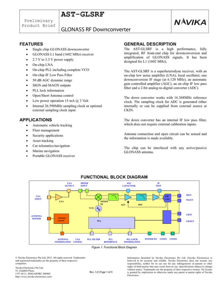
The AST-GLSRF is a superheterodyne receiver, with an
on-chip low noise amplifier (LNA), local oscillator, one
downconversion IF stage (at 6.120 MHz), an automatic
gain controlled amplifier (AGC), an on chip IF low pass
filter and a 2-bit analog-to-digital converter (ADC).
The down converter works with 16.368MHz reference
clock. The sampling clock for ADC is generated either
internally or can be supplied from external source at
CKIN.
APPLICATIONS
•
•
•
•
•
•
•
The down converter has an internal IF low pass filter,
which does not require external calibration inputs.
Automatic vehicle tracking
Fleet management
Security applications
Asset tracking
Car telematics/navigation
Marine navigation
Portable GLONASS receiver
Antenna connection and open circuit can be sensed and
the information is made available.
The chip can be interfaced with any active/passive
GLONASS antenna.
FUNCTIONAL BLOCK DIAGRAM
LNA
OUTPUT
MIXER
INPUT
AGC
CAPACITOR
IF
TEST
LNA
INPUT
ADC
2 bits
LNA
MIXER
IQ
AGC
SIGN
MAGN
BPF
VCO
ANTENNA
SENSOR
CKIN
Antenna
control
ANTENNA
INFORMATION
PLL
LNA
CONFIG
PLL FILTER
CKOUT
PLL
REFERENCE
PLL LOCK
INFORMATION
POWER ON
CONF1
CONF2
Figure 1. Functional Block Diagram
© Navika Electronics Pte Ltd, 2012. All rights reserved. Trademarks
and registered trademarks are the property of their respective
companies.
Navika Electronics Pte Ltd.
51, Goldhill Plaza,
# 07-10/11, SINGAPORE 308900
http://www.navika-electronics.com/
Rev. 1.0 | Page 1 of 4
Information furnished by Navika Electronics Pte Ltd. (Navika Electronics) is
believed to be accurate and reliable. Navika Electronics does not assume any
responsibility, neither for its use nor for any infringements of patents or other
rights of third parties that may result from its use. Specifications subject to change
without notice. Trademarks are the property of their respective owners. No license
is granted by implication or otherwise under any patent or patent rights of Navika
Electronics.
AST-GLSRF
Preliminary
Product Brief
GLONASS RF Front-end
PIN CONFIGURATION AND FUNCTION DESCRIPTIONS
Figure 2. Pin Configuration
PIN FUNCTION DESCRIPTIONS
Pin No.
1
2
3
4
5
6
7
8
9
10
11
12
13
14
15
16
Mnemonic
LNAOUT
ANT_INFO
CONF1
MIXINM
MIXINP
VCC_MIX
VCC_VCO
VTUNE
POWER_ON
PLL_LOCK
REF
VCC_PLL_ADC
CKOUT
MAGN
SIGN
VEE
Pin Type
Analog
Analog
CMOS
Analog
Analog
Supply
Supply
Analog
CMOS
Analog
Analog
Supply
CMOS
CMOS
CMOS
Ground
Input / Output
Output
Output
Input
Input
Input
17
18
19
20
IF_TEST
CAMP
VCC_IF
CLKIN
Analog
Analog
Supply
CMOS
Input
21
22
23
CONF2
LNAIN
ANT_SENSE
CMOS
Analog
Analog
Input
Input
Input
Input
Output
Input
Output
Output
Output
Output
Description
LNA RF Signal, (1597 – 1606 MHz)
Antenna connection information pin
Configuration pin
Positive MIXER RF Signal, (1597 – 1606 MHz)
Negative MIXER RF Signal, (1597 – 1606 MHz)
MIXER Supply
VCO Supply
External PLL filter connection
Power-On mode pin
PLL LOCK information pin
Reference Clock
PLL/ADC Supply
Reference frequency
Magnitude Bit Data
Sign Bit Data
Paddle ground internal connection / redundant with exposed pad
(paddle)
IF test
Amplitude bit capacitor signal
IF Supply
Optional Sampling clock. Selectable with CONF1 and CONF2
combination
Configuration pin
LNA RF Signal, (1597 – 1606 MHz)
Antenna sense for connection control
Rev 1.0 | Page 2 of 4
AST-GLSRF
Preliminary
Product Brief
Pin No.
24
Mnemonic
VCC_LNA
GLONASS RF Front-end
Pin Type
Supply
Input / Output
Description
LNA Supply
Table 1. Pin Function Descriptions
PACKAGE INFORMATION
Figure 3. 24-Lead Lead Frame Chip Scale Package [LFCSP_VQ]
Dimensions shown in millimeters
ORDERING GUIDE
Model
AST-GLSRF
Operating Voltage
3.0 V
Temperature Range
−40°C to +85°C
Table 2. Ordering Guide
Rev 1.0 | Page 3 of 4
Package Description
24L LFCSP
4mmx4mmx0.85mm
Lead free part
Package Option
AST-GLSRF
Preliminary
Product Brief
GLONASS RF Front-end
APPLICATION SCHEMATIC
VCC_LNA
VCC_MIX
VCC_VCO
VCC_IF
VCC_PLL_ADC
VCC_LNA
BPF
IF TEST
ADC
2 bits
LNA
MIXER
IQ
AGC
BPF
VCO
Antenna
control
PLL
VCC_ANT
TCXO
Digital interface
Figure 4. Application schematic
Rev 1.0 | Page 4 of 4
