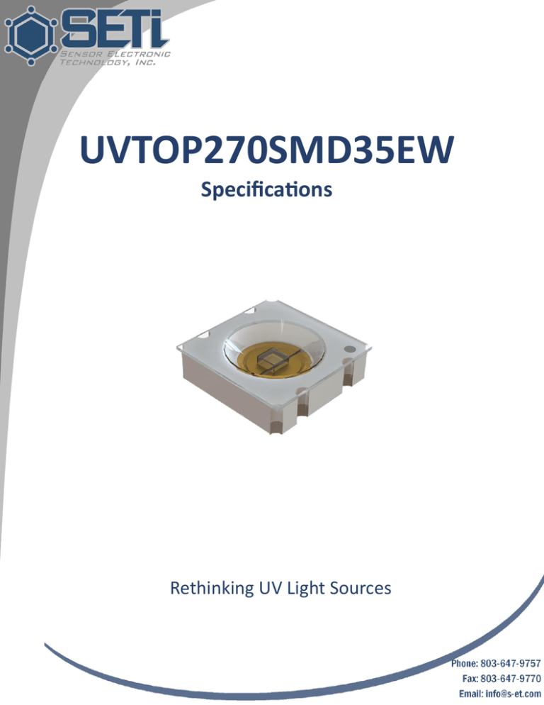
UVTOP270SMD35EW
Specifica ons
Rethinking UV Light Sources
Phone: 803-647-9757
Fax: 803-647-9770
Email: info@s-et.com
UVTOP270SMD35EW Specifica
ons
Table of Contents
Mechanical Dimensions………………………………. 2
LED Characteris cs……………………………………… 3
Characteris c Diagrams………………………………. 4 - 6
Angular Diagram ………………………………………... 7
Soldering Condi ons and Precau ons ………… 8
Precau ons for use…………………………………….. 9
Revision History………………………………………….. 10
Copyright © 2014 Sensor Electronic Technology, Inc. All rights reserved. The information in this document is subject to change without notice.1
UVTOP® is a registered trademark of Sensor Electronic Technology, Inc.
2
Mechanical Dimensions
3.50
3.50
3.50
0.95
1-
1-
0.95
2+
2+
3.50
Encapsulant Layer
0.810
0.900
Connec on:
1-: Cathode
2+: Anode
Dimensions in mm
Tolerances: .XX = +/- .3; .XXX = +/- .1
Copyright © 2014 Sensor Electronic Technology, Inc. All rights reserved. The information in this document is subject to change without notice.2
UVTOP® is a registered trademark of Sensor Electronic Technology, Inc.
3
Characteris cs
Electro-Op cal Characteris cs
TA = 25oC, with external heat sink Rth(sp-a) ≤ 20 °C/W, Forward Current=20mA
Parameter
Symbol
Unit
Minimum
Typical
Maximum
Peak Wavelength
λp
nm
265
273
280
Radiant Flux
Φe
mW
1.0
1.3
Forward Voltage
VF
V
4.5
5.5
6.5
FWHM
Δλ
nm
12
15
Viewing Angle
2θ1/2
⁰
120
Thermal Resistance (Tj-Tsp)
Rth
⁰C/W
60
Absolute Maximum Ra ngs
TA = 25 oC
Parameter
Symbol
Unit
Value
Power Dissipa on
Pd
mW
195
Forward Current
IF
mA
30
Reverse Voltage
Vr
V
-6
Junc on Temperature
Tj
⁰C
41
Storage Temperature
Tstg
⁰C
-30…+100
Notes:
The exposure to the absolute maximum rated condi ons may affect device reliability
The stresses beyond those listed under absolute maximum ra ng may cause permanent damage to the device
Peak wavelength measurement tolerance is ± 2 nm
Op cal power output measurement tolerance is ± 10%
Forward voltage measurement tolerance is ± 2%
Rth(sp-a) defined as thermal resistance from solder point to ambient
Copyright © 2014 Sensor Electronic Technology, Inc. All rights reserved. The information in this document is subject to change without notice.
3
UVTOP® is a registered trademark of Sensor Electronic Technology, Inc.
4
www.s-et.com ● +1 (803) 647-9757 ● sales@s-et.com
Rela ve Spectral Power Distribu on
Typical spectral power distribu on, Ta=25 °C
Peak Wavelength VS. Forward Current
Typical peak wavelength vs. forward current, Ta=25 °C
Copyright © 2014 Sensor Electronic Technology, Inc. All rights reserved. The information in this document is subject to change without notice.4
5
25
UVTOP® is a registered trademark of Sensor Electronic Technology, Inc.
5
www.s-et.com ● +1 (803) 647-9757 ● sales@s-et.com
Forward Current VS. Forward Voltage
Typical forward current vs. forward voltage, Ta=25 °C
Rela ve Radiant Flux VS. Forward Current
Typical rela ve radiant flux vs. forward current, Ta=25 °C
Copyright © 2014 Sensor Electronic Technology, Inc. All rights reserved. The information in this document is subject to change without notice.5
4
UVTOP® is a registered trademark of Sensor Electronic Technology, Inc.
6
Op cal Power Dera ng Plot
Typical rela ve radiant flux vs. Junc on Temperature, If=20mA
Angular Diagram
Typical angular diagram perpendicular to n-contact, If=20mA
Copyright © 2014 Sensor Electronic Technology, Inc. All rights reserved. The information in this document is subject to change without notice.6
6
UVTOP® is a registered trademark of Sensor Electronic Technology, Inc.
7
UVTOP® SMD Soldering Condi ons and Handling
UVTOP® SMD LEDs reflow characteris cs are compa ble with JEDEC J-STD-020C . It is generally recommended
to follow the solder profile provided by the manufacturer of the solder paste used. These profiles are suggested
as a guideline and may require adjustment depending on the users applica on.
It is recommended to verify the solder process through reflow of several test PCBs and subsequent X-ray or
shear tes ng of the devices. The solder should show minimum indica on of voids or solder grains.
Profile Parameters
Average Ramp-Up Rate (Tsmax to Tp)
Preheat: Temperature Min (Tsmin)
Preheat: Temperature Max (Tsmax)
Preheat: Time (tsmin to tsmax)
Time Maintained Above: Temperature (TL)
Time Maintained Above: Time (tL)
Peak/Classifica on Temperature (Tp)
Time Within 5 °C of Actual Peak Temperature (tp)
Ramp-Down Rate
Time 25 °C to Peak Temperature
Lead-based Solder
Lead-free Solder
3 °C/second max.
100 °C
150 °C
3 °C/second max.
150 °C
200 °C
60-120 seconds
60-180 seconds
183 °C
217 °C
60-90 seconds
60-90 seconds
215 °C
228 °C
10-30 seconds
20-40 seconds
6 °C/second max.
6 °C/second max.
6 minutes max.
8 minutes max.
A “no clean” solder paste is recommended so that cleaning is not required a er the solder reflow. The choice of
applica on method will determine the specific amount of solder, but for consistent results a solder stencil printer
or automated dispense system is suggested.
28
28
If cleaning a er reflow is required, isopropyl alcohol or water is recommended. Do not use ultrasonic cleaning.
Do not wave solder or hand solder UVTOP® SMD LEDs.
Copyright © 2014 Sensor Electronic Technology, Inc. All rights reserved. The information in this document is subject to change without notice.8
UVTOP® is a registered trademark of Sensor Electronic Technology, Inc.
8
Tape and Reel
All SETi carrier tapes conform to EIA-481, Automated Component Handling Systems Standard.
All dimensions in mm.
13”
Copyright © 2014 Sensor Electronic Technology, Inc. All rights reserved. The information in this document is subject to change without notice.
UVTOP® is a registered trademark of Sensor Electronic Technology, Inc.
9
Cau ons
UV Light
These devices are ultraviolet LEDs. During opera on, the LED emits high intensity ultraviolet (UV) light, which is
harmful to skin and eyes.
UV light is hazardous to skin and may cause cancer. Avoid exposure to UV light when LED is opera onal.
Precau ons must be taken to avoid looking directly at the UV light without the use of UV light protec ve glasses. Do
not look directly at the front of the LED or at the LED’s lens when LED is opera onal.
A ach the following warning labels on products/systems that use UV LEDs.
Sta c Electricity
These products are ESD (electrosta c discharge) sensi ve; sta c electricity and surge voltages seriously damage UV LEDs and can
result in complete failure of the device. Precau ons must be taken against ESD when handling or opera ng these devices.
Opera ng Condi ons
In order to ensure the correct func oning of these LEDs, compliance to the maximum electrical specifica ons is paramount.
These LEDs are par cularly sensi ve to any current value that exceeds the absolute maximum ra ng of the product. Any applied
current in excess of the maximum specifica on will cause damage and possible complete failure of the product.
The current flowing in a LED is an exponen al func on of the voltage across it. A small change in voltage can produce a very
large change in current and lead to complete failure of the LED. The use of current regulated drive circuits are recommended for
these products.
Any a empt to drive these UV LEDs with a voltage source instead of a current source will cause damage and possible complete failure of the product.
These LEDs are suscep ble to heat genera on. Use care to design end product with adequate thermal management
to ensure that LEDs do not exceed maximum recommended temperatures. Opera ng LEDs at temperatures in excess of specifica on will result in damage and possible complete failure of the product.
Copyright © 2014 Sensor Electronic Technology, Inc. All rights reserved. The information in this document is subject to change without notice.9
UVTOP® is a registered trademark of Sensor Electronic Technology, Inc.
10
Revision History
Revision
Change Date
Authorized Signature
00
August 11, 2014
Philip Krzyzaniak
01
October 14, 2014
Philip Krzyzaniak
Copyright © 2014 Sensor Electronic Technology, Inc. All rights reserved. The information in this document is subject to change without notice.10
UVTOP® is a registered trademark of Sensor Electronic Technology, Inc.
11


