Freescale Semiconductor
Application Note
AN1988
Rev 1, 05/2005
±1.5g Dual Axis Micromachined
Accelerometer Power Supply Rejection
Ratio (PSRR) Suggestions
by: Peter Schultz
Product Engineer
COMPONENT DESCRIPTION
The MMA6200Q series is a two axis (X and Y)
accelerometer family with sensitivity parallel to the device’s
mounting plane. The device utilizes variable capacitance
sensing elements and a two-channel interface IC all in a
16-pin QFN package.
This section provides a general description of the device
power supply rejection ratio (PSRR), how it affects device
performance, and suggestions for improvement.
INTRODUCTION TO POWER SUPPLY
Rejection Ratio
The power supply rejection ratio is a measure of how well
the device rejects the noise on the power supply line. The
MMA6200Q series is capable of being used in several
different applications. In some cases it may be possible for
supply line noise to adversely affect the output signal. This
phenomenon can create large output signals when the supply
line noise frequencies are roughly equal to the device’s
oscillator frequency and/or harmonics. The oscillator drives
the g-cell sampling as well as the internal low pass filter. When
the difference between the frequency of the noise on the
supply and the oscillator frequency is less than the low pass
filter cutoff frequency the aliased signal passes through the
filter. This aliased signal is then amplified internally by the
device creating an even more adverse effect. This noise at the
output can be as much as ten times the amplitude of the input
noise at the oscillator frequency or its harmonics.
IMPROVING THE POWER SUPPLY
Rejection Ratio
If the power supply contains noise approaching the
oscillator frequency, large amounts of noise may be observed
at the output of the device. This does not become an issue
until the noise frequency is a little larger than the oscillator
frequency; a little larger here meaning still within the internal
low pass filter’s bandwidth. In application a simple low pass
© Freescale Semiconductor, Inc., 2005. All rights reserved.
filter at the input helped to resolve this issue by attenuating
much of the offending noise before it enters the device.
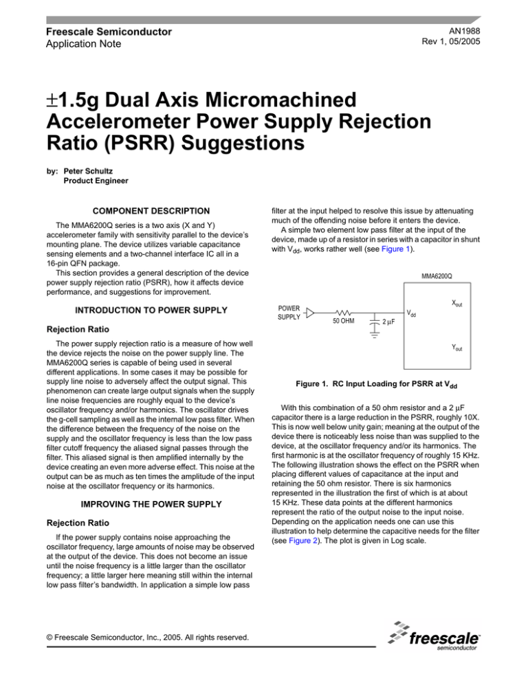
A simple two element low pass filter at the input of the
device, made up of a resistor in series with a capacitor in shunt
with Vdd, works rather well (see Figure 1).
MMA6200Q
POWER
SUPPLY
Xout
50 OHM
2 µF
Vdd
Yout
Figure 1. RC Input Loading for PSRR at Vdd
With this combination of a 50 ohm resistor and a 2 µF
capacitor there is a large reduction in the PSRR, roughly 10X.
This is now well below unity gain; meaning at the output of the
device there is noticeably less noise than was supplied to the
device, at the oscillator frequency and/or its harmonics. The
first harmonic is at the oscillator frequency of roughly 15 KHz.
The following illustration shows the effect on the PSRR when
placing different values of capacitance at the input and
retaining the 50 ohm resistor. There is six harmonics
represented in the illustration the first of which is at about
15 KHz. These data points at the different harmonics
represent the ratio of the output noise to the input noise.
Depending on the application needs one can use this
illustration to help determine the capacitive needs for the filter
(see Figure 2). The plot is given in Log scale.
Figure 2. PSRR with 50 Ohm and Varying Input Capacitance
One can see the PSRR has improved by roughly a factor of
10 with a 2 µF capacitor at the input. Not only can the plot be
used as a guide in the design of an input filter, it can also help
put in perspective the possible amplitudes of the signal and
about what frequencies they may occur. From looking at the
plot one can see that for a capacitance of 1uF the gains at the
two most predominate noise frequencies is unity. This means
the aliased signals will not be larger in amplitude than the input
noise that created it; giving the recommended smaller
capacitance filter in the following illustration (see Figure 3).
Xout
50 OHM
1 µF
MMA6200Q
POWER
SUPPLY
MMA6200Q
POWER
SUPPLY
If the series resistance and/or reactance is increased the
amount of noise at the output will be decreased. The series
reactance can be increased with the use of an inductor in
series with the resistor (see Figure 4). This is more
advantageous then adding more resistance due to the fact
that it does not produce a large DC voltage drop.
Vdd
Yout
Figure 3. Recommended RC Input Loading
for PSRR at Vdd
With cost as one of the deciding factors, this is a
recommended filter design for reducing the PSRR. One
should note however that variations in the individual devices
and the different axes of the device produce plots that may
look significantly different. The intent here is only to give an
idea of the effects of different capacitances on the oscillator
induced frequency gains. One must also remember to absorb
any impedance the source may have into the RC filter as the
source will also add its own impedance to the network.
Xout
50 OHM 1 mH
1 µF
Vdd
Yout
Figure 4. Recommended RCL Input Loading
for PSRR at Vdd
The device was designed to operate with 3.3 Vdc at Vdd. If
this input voltage is allowed to drop by more than half a volt
the device may not operate correctly; hence the use of an
inductor. With the use of an application board there was found
to be greater than a factor of two drop in the output noise at
the first harmonic with the use of the 1 mH inductor. The later
harmonics incur a larger improvement due to the higher
reactance of the inductor at the higher frequencies. As a result
there was greater than a factor of eight improvement with the
third and fifth harmonics. This RC and RLC circuit produced
the following PSRR plot (see Figure 5).
AN1988
2
Sensors
Freescale Semiconductor
Figure 5. PSRR with RC and RLC Input Filter
If a smaller capacitance is desired in application with no
inductor one can increase the value of just the series resistor.
However one must take into consideration the tradeoffs
involved. In order to get roughly the same improvement in the
PSRR with a 0.5 µF capacitor as there was with the 50 ohm
and 2 µF RC combination one must increase the series
impedence to 150 ohms (see Figure 6).
This alternate RC circuit produces the following effect on
the PSRR (see Figure 7). Notice the similarity in the gain when
compared with the 50 ohm 2 µF filter. It is still well below unity
for this configuration.
MMA6200Q
POWER
SUPPLY
Xout
150 OHM
0.5 µF
Vdd
Yout
Figure 6. Alternate RC Input Loading for PSRR at Vdd
Figure 7. PSRR with 150 Ohm and 0.5 µF Input Capacitance
AN1988
Sensors
Freescale Semiconductor
3
As stated before this large value of resistance creates a DC
voltage drop at the input of the device. However, it could be
reduced some and still achieve less than unity gain. With the
same voltage at the input of the filter the output voltage of the
device is lowered. In this case it drops by roughly 5 percent. In
turn, this loss in DC voltage also lowers the ratio-metric error.
However if the voltage at Vdd is allowed to drop much lower
than 2.7 volts the device may not operate at all. If cost and
space permits, one should consider, as stated previously, the
substitution of a series inductor in place of at least part of this
series resistance. This can greatly decrease the DC voltage
drop problem.
To get a 150 ohm impedance at the frequency of the first
harmonic we have X = 2*pie*(15 KHz)*L = 150 ohm. Solving
for L gives the somewhat large value of 1.6 mH for the
inductor. A 1 mH inductor at 15 KHz has an impedance of
about 95 ohms and these devices can be had in quantity
(1000 or more) for less then twenty cents each.
CONCLUSION
The MMA6200Q series family of devices require external
RC and possibly L components to correct power supply
rejection ratio issues caused by noisy power supply lines. This
may not be of concern in many applications; however, it may
be in some. The preceding gives an introduction to power
supply rejection ratio as well as some information to better
understand this potential problem. Also included are some
example filters, the effects on PSRR, as well as suggested
choices.
AN1988
4
Sensors
Freescale Semiconductor
NOTES
AN1988
Sensors
Freescale Semiconductor
5
NOTES
AN1988
6
Sensors
Freescale Semiconductor
NOTES
AN1988
Sensors
Freescale Semiconductor
7
How to Reach Us:
Home Page:
www.freescale.com
E-mail:
support@freescale.com
USA/Europe or Locations Not Listed:
Freescale Semiconductor
Technical Information Center, CH370
1300 N. Alma School Road
Chandler, Arizona 85224
+1-800-521-6274 or +1-480-768-2130
support@freescale.com
Europe, Middle East, and Africa:
Freescale Halbleiter Deutschland GmbH
Technical Information Center
Schatzbogen 7
81829 Muenchen, Germany
+44 1296 380 456 (English)
+46 8 52200080 (English)
+49 89 92103 559 (German)
+33 1 69 35 48 48 (French)
support@freescale.com
Japan:
Freescale Semiconductor Japan Ltd.
Headquarters
ARCO Tower 15F
1-8-1, Shimo-Meguro, Meguro-ku,
Tokyo 153-0064
Japan
0120 191014 or +81 3 5437 9125
support.japan@freescale.com
Asia/Pacific:
Freescale Semiconductor Hong Kong Ltd.
Technical Information Center
2 Dai King Street
Tai Po Industrial Estate
Tai Po, N.T., Hong Kong
+800 2666 8080
support.asia@freescale.com
For Literature Requests Only:
Freescale Semiconductor Literature Distribution Center
P.O. Box 5405
Denver, Colorado 80217
1-800-441-2447 or 303-675-2140
Fax: 303-675-2150
LDCForFreescaleSemiconductor@hibbertgroup.com
AN1988
Rev. 1
05/2005
Information in this document is provided solely to enable system and software
implementers to use Freescale Semiconductor products. There are no express or
implied copyright licenses granted hereunder to design or fabricate any integrated
circuits or integrated circuits based on the information in this document.
Freescale Semiconductor reserves the right to make changes without further notice to
any products herein. Freescale Semiconductor makes no warranty, representation or
guarantee regarding the suitability of its products for any particular purpose, nor does
Freescale Semiconductor assume any liability arising out of the application or use of any
product or circuit, and specifically disclaims any and all liability, including without
limitation consequential or incidental damages. “Typical” parameters that may be
provided in Freescale Semiconductor data sheets and/or specifications can and do vary
in different applications and actual performance may vary over time. All operating
parameters, including “Typicals”, must be validated for each customer application by
customer’s technical experts. Freescale Semiconductor does not convey any license
under its patent rights nor the rights of others. Freescale Semiconductor products are
not designed, intended, or authorized for use as components in systems intended for
surgical implant into the body, or other applications intended to support or sustain life,
or for any other application in which the failure of the Freescale Semiconductor product
could create a situation where personal injury or death may occur. Should Buyer
purchase or use Freescale Semiconductor products for any such unintended or
unauthorized application, Buyer shall indemnify and hold Freescale Semiconductor and
its officers, employees, subsidiaries, affiliates, and distributors harmless against all
claims, costs, damages, and expenses, and reasonable attorney fees arising out of,
directly or indirectly, any claim of personal injury or death associated with such
unintended or unauthorized use, even if such claim alleges that Freescale
Semiconductor was negligent regarding the design or manufacture of the part.
Freescale™ and the Freescale logo are trademarks of Freescale Semiconductor, Inc.
All other product or service names are the property of their respective owners.
© Freescale Semiconductor, Inc. 2005. All rights reserved.
