PD7500
Pulse-Width-Modulation Control Circuits
Description
The PD7500 is a voltage mode pulse width modulation switching regulator control circuit designed primarily for power supply
control.
The PD7500 consists of a reference voltage circuit, two error amplifies, an on-chip adjustable oscillator, a dead-time
control(DTC) comparator, a pulse-steering control flip-flop, and an output control circuit. The precision of voltage reference
(VREF) is improved up to ±1% through trimming and this provides a better output voltage regulation. The PD7500 provides for
push pull or single-ended output operation, which can be selected through the output control.
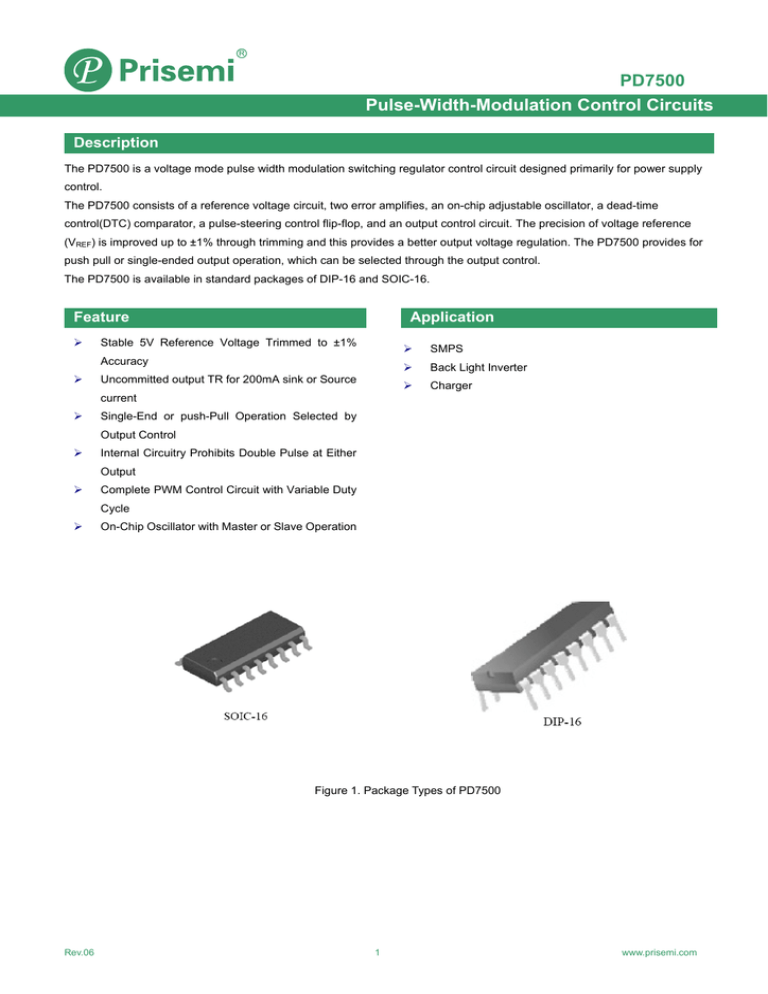
The PD7500 is available in standard packages of DIP-16 and SOIC-16.
Feature
Application
Stable 5V Reference Voltage Trimmed to ±1%
Accuracy
Uncommitted output TR for 200mA sink or Source
SMPS
Back Light Inverter
Charger
current
Single-End or push-Pull Operation Selected by
Output Control
Internal Circuitry Prohibits Double Pulse at Either
Output
Complete PWM Control Circuit with Variable Duty
Cycle
On-Chip Oscillator with Master or Slave Operation
Figure 1. Package Types of PD7500
Rev.06
1
www.prisemi.com
Pulse-Width-Modulation Control Circuits
PD7500
Pulse-Width-Modulation Control Circuits
Pin Configuration
P Package
(DIP-16)
M Package
(SOIC-16)
1IN+
1
16
2IN+
1IN+
1
16
2IN+
1IN-
2
15
2IN-
1IN-
2
15
2IN-
Feedback
3
14
Ref
Feedback
3
14
Ref
DTC
4
13
Output Ctrl
DTC
4
13
Output Ctrl
CT
5
12
VCC
CT
5
12
VCC
RT
6
11
C2
RT
6
11
C2
GND
7
10
E2
GND
7
10
E2
C1
8
9
E1
C1
8
9
E1
Figure 2. Pin Configuration of PD7500 (Top View)
Output Function Control Table
Signal for Output Control
Output Function
VI=GND
Single-ended or parallel output
VI=VREF
Normal push-pull operation
Functional Block Diagram
Output Ctrl
6
RT
5
CT
13
Oscillator
Flip-Flop
Dead-Time Control
DTC
-
4
Comparator
Error Amplifier 1
1IN+ 1
2
1IN-
2IN+
2IN-
FEEDBACK
D
+
0.12V
16
15
8 C1
Pulse-Steering
>CK
Q1
9
E1
C2
11
Q2
+
+
PWM
-
Comparator
10
12
+
-
Reference
Regulator
0.7mA
14
E2
VCC
REF
7 GND
3
Figure 3. Functional Block Diagram of PD7500
Rev.06
2
www.prisemi.com
Pulse-Width-Modulation Control Circuits
PD7500
Pulse-Width-Modulation Control Circuits
Absolute maximum rating (Note 1)
Parameter
Symbol
Value
Unit
Supply Voltage(Note 2)
VCC
40
V
Amplifier Input Voltage
VI
-0.3 to VCC+0.3
V
Collector Output Voltage
VO
40
V
Collector Output Current
IO
250
mA
Package Thermal Impedance (Note 3)
RθJA
M Package
73
P Package
67
Lead Temperature 1.6mm from case for
10 seconds
Storage Temperature Range
TSTG
ESD rating (Machine Model)
℃/W
260
℃
-65 to 150
℃
200
V
Note 1: Stresses greater than those listed under "Absolute Maximum Ratings" may cause permanent damage to the device.
These are stress ratings only, and functional operation of the device at these or any other conditions beyond those indicated
under "Recommended Operating Conditions" is not implied. Exposure to "Absolute Maximum Ratings"for extended periods
may affect device reliability.
Note 2: All voltage values are with respect to the network ground terminal.
Note 3: Maximum power dissipation is a function of TJ(max), RθJA and TA. The maximum allowable power dissipation at any
allowable ambient temperature is PD = ( TJ(max) - TA )/RθJA. Operating at the absolute maximum TJ of 150℃ can affect
reliability.
Recommended Operating Conditions
Parameter
Supply Voltage
Collector Output Voltage
Collector Output Current
(Each Transistor)
Symbol
Min
Typ
Max
Unit
VCC
7
15
36
V
30
36
V
200
mA
VCC-2
V
VC1,VC2
IC1,IC2
Amplifier Input Voltage
VI
0.3
Current Into Feedback Terminal
IFB
0.3
mA
Reference Output Current
IREF
10
mA
Timing Capacitor
CT
0.00047
0.001
10
μF
Timing Resistor
RT
1.8
30
500
KΩ
Oscillator Frequency
fosc
1.0
40
200
KHz
0.3
5.3
V
-40
85
℃
PWM Input Voltage(Pin3,4,and 13)
Operating Free-Air Temperature
Rev.06
TA
3
www.prisemi.com
Pulse-Width-Modulation Control Circuits
PD7500
Pulse-Width-Modulation Control Circuits
Electrical Characteristics
TA=25℃,VCC=20V,f=10KHz unless otherwise noted
Parameter
Symbol
Conditions
Min.
Typ.
Max.
Unit
IREF=1mA
4.75
5.0
5.25
V
IREF=1mA,TA=-40 to 85℃
4.7
5.0
5.2
V
Reference Section
Output Reference Voltage
VREF
Line Regulation
RLINE
VCC=7V to 36V
2
25
mV
Load Regulation
RLOAD
IREF=1mA to 10mA
1
15
mV
35
50
mA
Short-Circuit Output Current
ISC
VREF=0V
10
Oscillator Section
CT=0.001μF,RT=30 KΩ
CT=0.01μF,RT=12 KΩ
Oscillator Frequency
9.2
10
10.8
fosc
KHz
CT=0.01μF,RT=12 KΩ,
TA=-40 to 85℃
Frequency Change with Temperature
40
△f/△T
9.0
12
CT=0.01μF,RT=12 KΩ,
TA=-40 to 85℃
2
%
-10
μA
Dead-Time Control Section
Input Bias Current
Maximum Duty Cycle
IBIAS
D(MAX)
VCC=15V,V4=0 to 5.25V
VCC=15V,V4=0V,
Vpin13=VREF
-2
45
Zero Duty Cycle
Input Threshold Voltage
VITH
%
3
3.3
V
Maximum Duty Cycle
0
Error-Amplifier Section
Input Offset Voltage
VIO
Vpin3=2.5V
2
10
mV
Input Offset Current
IIO
Vpin3=2.5V
25
250
nA
Input Bias Current
IBIAS
Vpin3=2.5V
0.2
1
μA
Common-Mode Input Voltage Range
VCM
VCC=7V to 36V
VCC-2
V
Open-Loop Voltage Gain
GVO
VO=0.5V to 3.5V
Unity-Gain Bandwidth
BW
Common-Mode Rejection Ratio
CMRR
Output Sink Current (Feedback)
ISINK
Output Soure Current(Feedback)
ISOURCE
Rev.06
VID=-15mV to -5V,
Vpin3=0.7V
VID=15mV to 5V
Vpin3=3.5V
4
-0.3
70
95
dB
650
KHz
65
80
dB
-0.3
-0.7
mA
2
mA
www.prisemi.com
Pulse-Width-Modulation Control Circuits
PD7500
Pulse-Width-Modulation Control Circuits
Electrical Characteristics(Continued)
Parameter
Symbol
Conditions
Min.
Typ.
Max.
Unit
4
4.5
V
PWM Comparator Section
Input Threshold Voltage
VITH
Zeao duty Cycle
Input Sink Current
ISINK
Vpin3=0.7V
-0.3
-0.7
mA
Output Section
Common
Output Saturation
Voltage
VCE(SAT)
Emitter
VE=0V,IC=200mA
1.1
1.3
V
Emitter
VCC(SAT)
Follower
VCC=15V
1.5
2.5
2
100
μA
-100
μA
6
10
mA
100
200
ns
25
100
ns
IE=-200mA
Collector Off-State Current
IC(OFF)
VCE=36V,VCC=36V
Emitter Off-State Current
IE(OFF)
VCC=VC=36V,VE=0
Total Device
Supply Current
ICC
Vpin6=VREF,VCC=15V
Output Switching Characteristics
Rise Time
tR
Fall Time
tF
Common Emitter
Common Collector
Common Emitter
Common Collector
Naming Rule
PD
7500 M
16
Prisemi Device
Package:
16:16 Lead
M:SOIC-16
7500 Series
P:DIP-16
Rev.06
5
www.prisemi.com
Pulse-Width-Modulation Control Circuits
PD7500
Pulse-Width-Modulation Control Circuits
Parameter Measurement information
VCC=20V
4
Test
3
Inputs
12KΩ 6
VCC
8
DTC
C1
Feedback
E1
RT
C2 11
E2 10
5 CT
0.01μF 1
1IN+
150Ω
150Ω
4W
4W
Output 1
9
Output 2
2 1IN16 2IN+
15 2IN-
50KΩ
13 Output Ctrl
GND
7
REF 14
Test Circuit
Voltage
VCC
at C1
0V
Voltage
VCC
at C2
0V
Voltage
at CT
Threshold Voltage
DTC
0V
Threshold Voltage
FEEDBACK
0.7V
Duty Cycle
0%
MAX
0%
Voltage Waveforms
Figure 4. Operational Test Circuit and Waveforms
Rev.06
6
www.prisemi.com
Pulse-Width-Modulation Control Circuits
PD7500
Pulse-Width-Modulation Control Circuits
Parameter Measurement information(Continued)
Amplifier Under Test
+
VI
FEEDBACK
-
+
Vref
-
Other Amplifier
Figure 5. Error Amplifier Characteristics
20V
68Ω 4W
tf
Each Output
tf
Output
Circuit
90%
90%
CL=15pF
(See Note A)
10%
10%
Note A:CL includes probe and jig capacitance
Figure 6. Common-Emitter Configuration
20V
Each Output
90%
90%
Circuit
Output
CL=15pF
68Ω 4W
10%
10%
tf
tf
(See Note A)
Note A: CL includes probe and jig capacitance.
Figure 7. Emitter-Follower Configuration
Rev.06
7
www.prisemi.com
Pulse-Width-Modulation Control Circuits
PD7500
Pulse-Width-Modulation Control Circuits
Typical Performance Characteristics
VCC=20V,
TA=25℃
0.001μF
10K
0.01μF
0.1μF
1K
1K
100K
10K
RT-Timing Resistance(Ω)
1M
Figure 8. Oscillator Frequency vs. RT and CT
100
VCC=20V,
△VO=3V
80
TA=25℃
60
40
20
0
1
10K
100
Frequency (Hz)
1M
Figure 9. Error Amplifier Small-Signal Voltage Gain vs. Frequency
Rev.06
8
www.prisemi.com
Pulse-Width-Modulation Control Circuits
PD7500
Pulse-Width-Modulation Control Circuits
Typical Applications
(VO=5V, IO=1A)
(VI=10V to 40V)
1mH 2A
KSA1010
VI (+)
VO
47
150
12
VCC
11
0.1μ
8
C2
C1
1M
5.1K
3
2
Feed
1IN-
Back
REF
2IN-
PD7500
1IN+
2IN+
14
15
+
5.1K
50μ
10V
5.1K
1
16
Output
DTC GND E1
4
9
7
Control
13
E2
RT
10
CT
6
5
47K
0.001μ
150
50μ
+
10V
GND
0.1
VI (-)
Figure 10.Pulse Width Modulated Step-Down Converter
Rev.06
9
www.prisemi.com
Pulse-Width-Modulation Control Circuits
PD7500
Pulse-Width-Modulation Control Circuits
Product dimension(SOIC-16)
Unit:mm(inch)
1.350(0.053)
1.750(0.069)
0.300(0.013)
0.510(0.020)
1.250(0.049)
1.650(0.065)
7°
A
20:1
0.250(0.010)
9.800(0.386)
10.200(0.402)
0°
8°
R0.200(0.008)
R0.200(0.008)
5.800(0.228)
6.240(0.246)
3.800(0.150)
4.040(0.159)
0.050(0.002)
0.250(0.010)
B
20:1
8°
9.5°
C
3°
7°
8°
8°
Rev.06
0.400(0.016)
1.270(0.050)
A
0.200(0.008)
SΦ1.000(0.039)
Depth 0.200(0.008)
0.200(0.008)
0.250(0.010)
C-C
50:1
1.000(0.039)
0.170(0.007)
0.250(0.010)
1.270(0.050)
BSC
B
C
0.400(0.016)×45°
10
www.prisemi.com
Pulse-Width-Modulation Control Circuits
PD7500
Pulse-Width-Modulation Control Circuits
Product dimension (DIP-16)
Unit:mm(inch)
6°
3.710(0.146)
4.310(0.170)
0.700(0.028)
7.320(0.288)
7.920(0.312)
5°
6°
1.524(0.060)TYP
3.200(0.126)
3.600(0.142)
4°
4°
0.360(0.014)
0.560(0.022)
2.540(0.100)
TYP
0.510(0.020)MIN
3.000(0.118)
3.600(0.142)
0.204(0.008)
0.360(0.014)
8.200(0.323)
9.400(0.370)
Φ3.000(0.118)
Depth
0.050(0.002)
0.150(0.006)
6.200(0.244)
6.600(0.260)
18.800(0.740)
19.200(0.756)
R0.750(0.030)
Rev.06
11
www.prisemi.com
Pulse-Width-Modulation Control Circuits
PD7500
Pulse-Width-Modulation Control Circuits
IMPORTANT NOTICE
and
are registered trademarks of Prisemi Electronics Co., Ltd (Prisemi) ,Prisemi
reserves the right to make changes without further notice to any products herein. Prisemi makes
no warranty, representation or guarantee regarding the suitability of its products for any particular
purpose, nor does Prisemi assume any liability arising out of the application or use of any
product or circuit, and specifically disclaims any and all liability, including without limitation
special, consequential or incidental damages. “Typical” parameters which may be provided in
Prisemi data sheets and/or specifications can and do vary in different applications and actual
performance may vary over time. All operating parameters, including “Typicals” must be
validated for each customer application by customer’s technical experts. Prisemi does not
convey any license under its patent rights nor the rights of others. The products listed in this
document are designed to be used with ordinary electronic equipment or devices, Should you
intend to use these products with equipment or devices which require an extremely high level of
reliability and the malfunction of with would directly endanger human life (such as medical
instruments, aerospace machinery, nuclear-reactor controllers, fuel controllers and other safety
devices), please be sure to consult with our sales representative in advance.
Website: http://www.prisemi.com
For additional information, please contact your local Sales Representative.
©Copyright 2009, Prisemi Electronics
is a registered trademark of Prisemi Electronics.
All rights are reserved.
Rev.06
12
www.prisemi.com


