Freescale Semiconductor
Order this document
by TPUPN17/D
Pulse Width Modulation TPU Function (PWM)
By Kevin Anderson
1 Functional Overview
Freescale Semiconductor, Inc...
This output function generates a pulse-width-modulated waveform in which the period and/or the high
time can be changed at any time by the CPU. PWM uses two modes of operation: level and normal. In
level mode, a 0% or a 100% duty-cycle waveform can be generated. In normal mode, waveforms with
duty-cycles between 0% and 100% can be generated.
In general, any changed period or high time is used in subsequent waveform synthesis, after a low-tohigh transition. An immediate update is possible in either mode. After an immediate update, the new
period and/or high time is reflected in the output waveform during the immediate host-service state, instead of waiting for a subsequent low-to-high transition.
2 Detailed Description
To start a PWM waveform, the CPU configures or updates parameters PWMPER (period desired) and
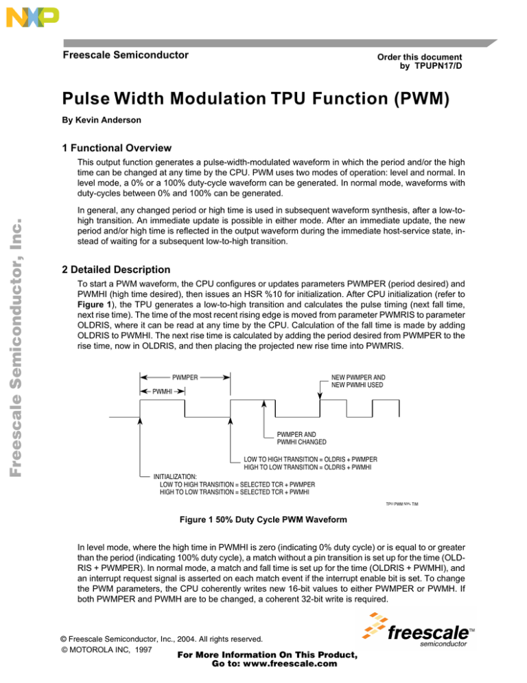
PWMHI (high time desired), then issues an HSR %10 for initialization. After CPU initialization (refer to
Figure 1), the TPU generates a low-to-high transition and calculates the pulse timing (next fall time,
next rise time). The time of the most recent rising edge is moved from parameter PWMRIS to parameter
OLDRIS, where it can be read at any time by the CPU. Calculation of the fall time is made by adding
OLDRIS to PWMHI. The next rise time is calculated by adding the period desired from PWMPER to the
rise time, now in OLDRIS, and then placing the projected new rise time into PWMRIS.
PWMPER
NEW PWMPER AND
NEW PWMHI USED
PWMHI
PWMPER AND
PWMHI CHANGED
LOW TO HIGH TRANSITION = OLDRIS + PWMPER
HIGH TO LOW TRANSITION = OLDRIS + PWMHI
INITIALIZATION:
LOW TO HIGH TRANSITION = SELECTED TCR + PWMPER
HIGH TO LOW TRANSITION = SELECTED TCR + PWMHI
TPU PWM 50% TIM
Figure 1 50% Duty Cycle PWM Waveform
In level mode, where the high time in PWMHI is zero (indicating 0% duty cycle) or is equal to or greater
than the period (indicating 100% duty cycle), a match without a pin transition is set up for the time (OLDRIS + PWMPER). In normal mode, a match and fall time is set up for the time (OLDRIS + PWMHI), and
an interrupt request signal is asserted on each match event if the interrupt enable bit is set. To change
the PWM parameters, the CPU coherently writes new 16-bit values to either PWMPER or PWMH. If
both PWMPER and PWMH are to be changed, a coherent 32-bit write is required.
© Freescale Semiconductor, Inc., 2004. All rights reserved.
© MOTOROLA INC, 1997
For More Information On This Product,
Go to: www.freescale.com
Freescale Semiconductor, Inc.
In both normal and level modes the new parameters are referenced to the next low-to-high transition.
An immediate update of either or both parameters may be selected by the CPU by issuing an HSR %01.
The immediate result to the waveform depends upon the point at which the immediate update is taken
(See 7 Performance and Use of Function).
A optional CPU interrupt request can be made at the beginning of each pulse in any mode or after an
immediate update. This allows the CPU to schedule parameter changes in relationship to a known point
in the waveform.
3 Function Code Size
Total TPU function code size determines what combination of functions can fit into a given ROM or emulation memory microcode space. PWM function code size is:
Freescale Semiconductor, Inc...
32 µ instructions + 8 entries = 40 long words
4 Function Parameters
This section provides detailed descriptions of function parameters stored in channel parameter RAM.
Figure 2 shows TPU parameter RAM address mapping. Figure 3 shows the parameter RAM assignment used by the function. In the diagrams, Y = M111, where M is the value of the module mapping bit
(MM) in the system integration module configuration register (Y = $7 or $F).
Channel
Base
Number
Address
0
1
2
Parameter Address
3
4
5
6
7
0
$YFFF##
00
02
04
06
08
0A
—
—
1
$YFFF##
10
12
14
16
18
1A
—
—
2
$YFFF##
20
22
24
26
28
2A
—
—
3
$YFFF##
30
32
34
36
38
3A
—
—
4
$YFFF##
40
42
44
46
48
4A
—
—
5
$YFFF##
50
52
54
56
58
5A
—
—
6
$YFFF##
60
62
64
66
68
6A
—
—
7
$YFFF##
70
72
74
76
78
7A
—
—
8
$YFFF##
80
82
84
86
88
8A
—
—
9
$YFFF##
90
92
94
96
98
9A
—
—
10
$YFFF##
A0
A2
A4
A6
A8
AA
—
—
11
$YFFF##
B0
B2
B4
B6
B8
BA
—
—
12
$YFFF##
C0
C2
C4
C6
C8
CA
—
—
13
$YFFF##
D0
D2
D4
D6
D8
DA
—
—
14
$YFFF##
E0
E2
E4
E6
E8
EA
EC
EE
15
$YFFF##
F0
F2
F4
F6
F8
FA
FC
FE
— = Not Implemented (reads as $00)
Figure 2 TPU Channel Parameter RAM CPU Address Map
Figure 3 shows all of the host interface areas for the PWM function, as well as the parameters, addresses, reference times, and reference sources. This segment lists and defines the parameters for all modes
of the PWM time function.
2
For More Information On This Product,
Go to: www.freescale.com
TPU Programming Library
TPUPN17/D
Freescale Semiconductor, Inc.
15
14
13
12
11
10
9
8
7
6
5
4
3
2
1
0
CHANNEL_CONTROL
$YFFFW0
OLDRIS
$YFFFW2
$YFFFW4
PWMHI(1,3)
$YFFFW6
PWMPER(2,3)
$YFFFW8
PWMRIS
$YFFFWA
Y= Channel number
Parameter Write Access:
Written by CPU
Written by TPU
Freescale Semiconductor, Inc...
Written by CPU and TPU
Unused parameters
Figure 3 Function Parameter RAM Assignment
4.1 CHANNEL_CONTROL
CHANNEL_CONTROL contains the channel latch controls and configures the PSC, PAC, and TBS
fields. The PSC field forces the output level of the pin directly without affecting the PAC latches, or forces the output level to the state specified by the PAC latches. The PAC field specifies the pin logic response as either a timer channel input or output. The TBS field configures a channel pin as input or
output and configures the time base for output match/input capture events.
15
14
13
12
11
10
9
8
7
NOT USED
6
5
4
TBS
3
2
1
PAC
0
PSC
NOTE
This channel must be configured as an output because the PWM function is indeterminate when programmed as an input.
Table 1 CHANNEL_CONTROL Options
TBS
PAC
8765
432
1xx
01xx
0100
0111
11xx
PSC
Action
10
Input
Output
00
01
10
11
—
—
—
—
Force Pin as Specified by PAC
Latches
Force Pin High
Force Pin Low
Do Not Force Any State
Do Not Change PAC
Do Not Change PAC
—
—
—
Do Not Change TBS
Output Channel
Capture TCR1, Compare TCR1
Capture TCR2, Compare TCR2
Do Not Change TBS
The PSC field determines the setting of the pin after initialization. In normal mode, PSC is set to force
the pin high. In level mode, where a 0% duty cycle is desired, PSC should be set to force the pin low at
initialization. The PAC field specifies the pin logic response as a timer channel output; however, the
PWM function does not use the PAC field, but uses direct control by the microcode.
CHANNEL_CONTROL must be written by the CPU before initialization.
TPU Programming Library
TPUPN17/D
For More Information On This Product,
Go to: www.freescale.com
3
Freescale Semiconductor, Inc.
4.2 OLDRIS
OLDRIS is the time of the previous low-to-high transition. When executing state Init, the TPU sets OLDRIS to the value of either TCR1 or TCR2 as specified in CHANNEL_CONTROL. When PWM is executing in normal mode (PWMPER > PWMHI), the TPU updates OLDRIS at the beginning of each pulse to
the time of the last low-to-high transition.
4.3 PWMRIS
PWMRIS is the current calculated rise time calculated at the beginning of the pulse (on the low-to-high
transition) by adding OLDRIS to PWMPER. The TPU updates this parameter.
Freescale Semiconductor, Inc...
4.4 PWMHI
PWMHI, which is updated by the CPU, is the current pulse high time that may be updated at any time.
Estimate for best-case minimum value for PWMHI is greater than 32 system clocks, assuming a single
channel operating. When more than one channel is operating, the minimum value for PWMHI depends
on TPU configuration (the variables are described in 7 Performance and Use of Function). The maximum value is $8000. The user should calculate case timing to ensure proper execution of this function.
4.5 PWMPER
PWMPER, which is updated by the CPU, is the current PWM period and is used by the TPU to calculate
the next low-to-high transition time. Estimate for best-case minimum value for PWMPER is greater than
32 system clocks, assuming that a single channel is operating. When more than one channel is operating, the minimum value for PWMPER depends on TPU configuration (the variables are described in
7 Performance and Use of Function). The maximum usable value is that which satisfies the condition:
(PWMPER – PWMHI) is less than or equal to $8000. PWMHI and PWMPER must be accessed coherently. The user should calculate the case timing to ensure proper execution of this function. Normal,
100%, and 0% duty cycles are defined as follows.
0%
100%
Else normal
4
→
→
→
PWMHI = 0
PWMPER ≤ PWMHI, AND PWMHI ≠ 0
PWMPER > PWMHI, AND PWMHI ≠ 0
For More Information On This Product,
Go to: www.freescale.com
TPU Programming Library
TPUPN17/D
Freescale Semiconductor, Inc.
5 Host Interface to Function
This section provides information concerning the TPU host interface to the function. Figure 4 is a TPU
address map. Detailed TPU register diagrams follow the figure. In the diagrams, Y = M111, where M is
the value of the module mapping bit (MM) in the system integration module configuration register (Y =
$7 or $F).
Freescale Semiconductor, Inc...
Address
15
8
7
0
$YFFE00
TPU MODULE CONFIGURATION REGISTER (TPUMCR)
$YFFE02
TEST CONFIGURATION REGISTER (TCR)
$YFFE04
DEVELOPMENT SUPPORT CONTROL REGISTER (DSCR)
$YFFE06
DEVELOPMENT SUPPORT STATUS REGISTER (DSSR)
$YFFE08
TPU INTERRUPT CONFIGURATION REGISTER (TICR)
$YFFE0A
CHANNEL INTERRUPT ENABLE REGISTER (CIER)
$YFFE0C
CHANNEL FUNCTION SELECTION REGISTER 0 (CFSR0)
$YFFE0E
CHANNEL FUNCTION SELECTION REGISTER 1 (CFSR1)
$YFFE10
CHANNEL FUNCTION SELECTION REGISTER 2 (CFSR2)
$YFFE12
CHANNEL FUNCTION SELECTION REGISTER 3 (CFSR3)
$YFFE14
HOST SEQUENCE REGISTER 0 (HSQR0)
$YFFE16
HOST SEQUENCE REGISTER 1 (HSQR1)
$YFFE18
HOST SERVICE REQUEST REGISTER 0 (HSRR0)
$YFFE1A
HOST SERVICE REQUEST REGISTER 1 (HSRR1)
$YFFE1C
CHANNEL PRIORITY REGISTER 0 (CPR0)
$YFFE1E
CHANNEL PRIORITY REGISTER 1 (CPR1)
$YFFE20
CHANNEL INTERRUPT STATUS REGISTER (CISR)
$YFFE22
LINK REGISTER (LR)
$YFFE24
SERVICE GRANT LATCH REGISTER (SGLR)
$YFFE26
DECODED CHANNEL NUMBER REGISTER (DCNR)
Figure 4 TPU Address Map
CIER — Channel Interrupt Enable Register
$YFFE0A
15
14
13
12
11
10
9
8
7
6
5
4
3
2
1
0
CH 15
CH 14
CH 13
CH 12
CH 11
CH 10
CH 9
CH 8
CH 7
CH 6
CH 5
CH 4
CH 3
CH 2
CH 1
CH 0
CH
Interrupt Enable
0
Channel interrupts disabled
1
Channel interrupts enabled
CFSR[0:3] — Channel Function Select Registers
15
14
13
12
CFS (CH 15, 11, 7, 3)
11
10
9
CFS (CH 14, 10, 6, 2)
$YFFE0C – $YFFE12
8
7
6
5
4
CFS (CH 13, 9, 5, 1)
3
2
1
0
CFS (CH 12, 8, 4, 0)
CFS[4:0] — PWM Function Number (Assigned during microcode assembly)
TPU Programming Library
TPUPN17/D
For More Information On This Product,
Go to: www.freescale.com
5
Freescale Semiconductor, Inc.
HSQR[0:1] — Host Sequence Registers
14
15
CH 15, 7
13
12
CH 14, 6
11
$YFFE14 – $YFFE16
10
9
CH 13, 5
8
7
CH 12, 4
6
5
CH 11, 3
4
3
CH 10, 2
CH[15:0]
Action Taken
xx
Not used in this function.
14
Freescale Semiconductor, Inc...
CH 15, 7
13
12
CH 14, 6
11
10
9
CH 13, 5
14
CH 15, 7
13
12
CH 14, 6
8
7
CH 12, 4
6
5
CH 11, 3
4
3
CH 10, 2
CH 8, 0
2
1
CH 9, 1
CH[15:0]
Initialization
00
No Host Service (Reset Condition)
01
Immediate Update
10
Initialization
11
Undefined
11
0
$YFFE18 – $YFFE1A
CPR[1:0] — Channel Priority Registers
15
1
CH 9, 1
HSRR[0:1] — Host Service Request Registers
15
2
0
CH 8, 0
$YFFE1C – $YFFE1E
10
9
CH 13, 5
8
7
CH 12, 4
6
5
CH 11, 3
4
3
CH 10, 2
CH[15:0]
Channel Priority
00
Disabled
01
Low
10
Middle
11
High
2
1
CH 9, 1
0
CH 8, 0
CISR — Channel Interrupt Status Register
$YFFE20
15
14
13
12
11
10
9
8
7
6
5
4
3
2
1
0
CH 15
CH 14
CH 13
CH 12
CH 11
CH 10
CH 9
CH 8
CH 7
CH 6
CH 5
CH 4
CH 3
CH 2
CH 1
CH 0
CH
Interrupt Status
0
Channel interrupt not asserted
1
Channel interrupt asserted
6 Function Configuration
The CPU initializes this time function by the following:
1. Writing CHANNEL_CONTROL, PWMHI, and PWMPER to RAM;
2. Issuing an HSR %10 for initialization; and
3. Enabling channel servicing by assigning a high, middle, or low priority.
The TPU then executes initialization and asserts an interrupt if the interrupt enable bit is set. In the beginning of each period, new pulse parameters are calculated and interrupts are attempted. The CPU
should monitor the HSR register (or the channel interrupt) until the TPU clears the service request to 00
before changing any parameters or issuing a new service request to this channel.
6
For More Information On This Product,
Go to: www.freescale.com
TPU Programming Library
TPUPN17/D
Freescale Semiconductor, Inc.
In normal mode (PWMPER > PWMHI), the TPU stores the time of the last low-to-high transition in OLDRIS, which can be read by the CPU. The TPU calculates the pulse timing (next fall time, next rise time)
in the beginning of the pulse, after generating a low-to-high transition. An interrupt is then asserted if
the interrupt enable bit is set. To change the PWM parameters, the CPU writes PWMPER and/or PWMHI to the parameter RAM. The two parameters must be written as 16-bit values.
Generally, the new parameters are referenced on the next low-to-high transition. For an immediate update of the waveform, the CPU issues HSR %01, which can be issued whenever any previous service
request has been serviced, indicated by the HSR bits of the channel at 00. When immediate update is
executed, the TPU asserts an interrupt if the interrupt enable bit is set. After issuing either HSR %01 or
HSR %10, the CPU should wait for the HSR bits to be cleared by the TPU before changing any parameters or issuing another service request to the channel.
Freescale Semiconductor, Inc...
Table 2 Host Service Request Bit Encoding
CH[1:0]
Action Taken
00
No Host Service Request
01
Immediate Update
10
Initialization
11
Undefined
7 Performance and Use of Function
7.1 Performance
Like all TPU functions, PWM function performance in an application is to some extent dependent upon
the service time (latency) of other active TPU channels. This is due to the operational nature of the
scheduler. When a single PWM channel is in use and no other TPU channels are active, the minimum
time between any two pulse edges is greater than 32 CPU clocks. When more TPU channels are active,
performance decreases. However, worst-case latency in any TPU application can be closely estimated.
To analyze the performance of an application that appears to approach the limits of the TPU, use the
guidelines given in the TPU reference manual and the information in the PWM state timing table below.
Table 3 Pulse Width Modulation Function — State Timing
State Number & Name
Max. CPU Clock Cycles
RAM Accesses by TPU
S1 Init
32
4
S2 Normal_L_H
24
4
S3 Normal_H_L
2
1
S4 Normal_0
24
4
S5 Immed_H
28
3
S6 Immed_L
28
3
7.2 Changing Duty Cycle
The CPU can change the duty cycle at any time once the TPU has completed the initialization state
(indicated by HSR %00 or a CPU interrupt request). Changes are made by writing a new high time value
to PWMHI in the channel's parameter RAM.
The minimum duty cycle (and the maximum non-100% duty cycle) is dependent on the number of active
TPU channels and the maximum channel latency as discussed above. A 0% duty cycle is generated by
setting PWMHI = 0. A 100% duty cycle is scheduled by setting PWMPER less than or equal to PWMHI
when PWMHI is not equal to zero.
TPU Programming Library
TPUPN17/D
For More Information On This Product,
Go to: www.freescale.com
7
Freescale Semiconductor, Inc.
Duty cycle changes take effect at the completion of the current period unless an immediate update
(HSR %01) is also requested. Immediate updates may be requested for any duty cycle including 0%
and 100%. A new PWMHI value with an immediate update HSR causes the TPU to change the currently
scheduled high-to-low time. This can cause the undesired side effect of an improper duty cycle for one
period. Figure 5 is an example of such a case.
In Figure 5 the newly requested duty cycle is shorter than the current one. When the immediate HSR
is serviced, the TPU schedules a new high-to-low transition time. However, this new value is less than
the current TCR value, so that the TPU greater-than-or-equal-to comparator fires, generating an immediate high-to-low transition. At the end of the period, the new high time is again used to calculate the
next falling edge, with reference to the latest rise time — from this point, the duty cycle is correct.
PWMPER
Freescale Semiconductor, Inc...
OLD PWMHI
NEITHER
NEW PWMHI
PWMHI CHANGED WITH
IMMEDIATE UPDATE
TPU PWM C UP W/ TIM
Figure 5 Immediate Duty Cycle Update With A One Period Anomaly
If the update in the above example happens at a point in the period that is before the newly specified
fall time, then the new duty cycle occurs as planned in the current cycle, with no intermediate glitches.
This is shown in Figure 6. If the update occurs at a time after the falling edge of the current pulse the
new duty cycle takes effect in the next period. This is shown in Figure 7.
PWMPER
OLD PWMHI
NEW PWMHI
PWMHI CHANGED WITH
IMMEDIATE UPDATE
TPU PWM C UP W/O TIM
Figure 6 Immediate Duty Cycle Update Without Anomaly
PWMPER
OLD PWMHI
NEW PWMHI
PWMHI CHANGED WITH
IMMEDIATE UPDATE
TPU PWM DEL CYC TIM
Figure 7 Immediate Duty Cycle Update Delayed One Period
Many applications are intolerant of the duty cycle glitch described above. For that reason the normal
update mode is preferred for most applications.
8
For More Information On This Product,
Go to: www.freescale.com
TPU Programming Library
TPUPN17/D
Freescale Semiconductor, Inc.
7.3 Changing Period
Once the TPU has completed the initialization state the CPU may at any time specify a new period by
writing to the PWMPER parameter. Unless the CPU also generates an immediate update service request the new period takes effect at the beginning of the next period, as shown in Figure 1. That is, a
new rise time is calculated at the next low-to-high transition. Thus, the current period is allowed to complete before the new one begins.
If an immediate update is requested in conjunction with a new period, the TPU immediately calculates
a new rise time that is applied during the current period. If the new period is longer than the old period
the new period takes effect immediately. If the new period is shorter than the old, the current period may
actually be shorter than the old period but longer than the new period. An example of this is shown in
Figure 8.
Freescale Semiconductor, Inc...
OLD PWMPER
NEITHER
OLD PWMHI
NEW PWMPER
NEW PWMHI
PWMPER AND PWMHI CHANGED
WITH IMMEDIATE UPDATE
TPU PWM P UP W/ TIM
Figure 8 Immediate Period Update With Single Period Anomaly
In this example a new PWMPER and PWMHI time have been requested at the time indicated. Since
the current pulse high time has expired, a shorter high time has no impact on this cycle. However, the
newly calculated low-to-high time (OLDRIS + PWMPER) is now less than the current time and the TPU
greater-than-or-equal-to comparator immediately generates the rising edge. At this point new high-tolow and low-to-high times are calculated and the new correct period and high time are in effect.
If the update had occurred earlier in the period the result would have been different. This is illustrated
in Figure 9. Here, the update occurs such that both the newly scheduled rising and falling edges are in
the future. Thus both will occur in the proper places and the one cycle anomaly is eliminated.
OLD PWMPER
OLD PWMHI
NEW PWMPER
NEW PWMHI
PWMPER AND PWMHI CHANGED
WITH IMMEDIATE UPDATE
TPU PWM P UP W/O TIM
Figure 9 Immediate Period Update With No Anomaly
Remember that updates made without using the immediate update feature always take effect on the
next rising edge and no anomalous behavior occurs. If an application requires both the period and high
time to be updated coherently, it is best to enable the CPU interrupt before the update. During the interrupt service the new period and high time can be updated. The interrupt occurs at the beginning of
the period, so as long as the interrupt service finishes before the end of the period, the new period and
high time take effect during the same cycle. Without this time reference, the parameter updates could
straddle the end of a period and one would take effect a cycle ahead of the other. This could cause the
single cycle anomalies discussed earlier.
TPU Programming Library
TPUPN17/D
For More Information On This Product,
Go to: www.freescale.com
9
Freescale Semiconductor, Inc.
7.4 Counting Periods
The TPU generates a CPU interrupt service request during the channel service at the beginning of each
period. The CPU can respond to these requests to keep track of how many periods have elapsed. In
this way, new pulse widths can be scheduled at a known position in time.
7.5 Stopping the Function
Once PWM operation is initialized on a channel, it runs without CPU intervention until a reset occurs. If
it is necessary to turn off a PWM channel, the CPU can write zeros to the channel function select bits
in registers CFSR[0:3]. This disables the function on the channel. Another way to disable output is to
select 0% or 100% duty cycle in the channel parameter RAM. In this case the PWM continues to run
and receive channel service but no transitions are seen on the pin.
Freescale Semiconductor, Inc...
8 PWM Examples
The following examples give an indication of the capabilities of the PWM function. Each example includes a description of the example, a diagram of the initial parameter RAM content, initial control bit
settings, and a diagram of the output waveform.
8.1 Example A
8.1.1 Description
Generate a 50% duty cycle waveform with a period equal to $800 TCR1 clocks on channel 1.
8.1.2 Initialization
Disable channel 1 by clearing the priority bits (CPR1[3:2]). Select PWM function by programming the
function select register for channel 1 (CFSR3[7:4]). Configure the parameter RAM for channel 1 as
shown below. Write HSRR1[3:2] = %10 to initialize the channel on the first channel service. Write the
priority bits (CPR1[3:2] to high, medium, or low priority to begin channel service.
Table 4 PWM Channel Parameter RAM
15
8
0
$YFFF10
0
0
0
0
0
0
0
0
1
0
0
1
0
0
0
1
$YFFF12
x
x
x
x
x
x
x
x
x
x
x
x
x
x
x
x
CH_CNTL
$YFFF14
0
0
0
0
0
1
0
0
0
0
0
0
0
0
0
0
PWMHI
$YFFF16
0
0
0
0
1
0
0
0
0
0
0
0
0
0
0
0
PWMPER
$YFFF18
x
x
x
x
x
x
x
x
x
x
x
x
x
x
x
x
$YFFF1A
x
x
x
x
x
x
x
x
x
x
x
x
x
x
x
x
8.1.3 Output Waveforms
INITIALIZATION
TPU PWM EXA TIM
10
For More Information On This Product,
Go to: www.freescale.com
TPU Programming Library
TPUPN17/D
Freescale Semiconductor, Inc.
8.2 Example B
8.2.1 Description
The waveform in Example A is running on Channel 1. Change the duty cycle to 25% using normal update mode.
8.2.2 Initialization
Change the value in PWMHI as shown in below. The new duty cycle becomes effective in the period
following the update.
Table 5 PWM Channel Parameter RAM
15
8
Freescale Semiconductor, Inc...
$YFFF10
$YFFF12
$YFFF14
0
UNCHANGED
CH_CNTL
UNCHANGED
0
0
0
0
0
0
1
0
0
OLDRIS
0
0
0
0
0
0
0
PWMHI
$YFFF16
UNCHANGED
PWMPER
$YFFF18
UNCHANGED
PWMRIS
$YFFF1A
UNCHANGED
8.2.3 Output Waveforms
PWMHI = $200
TPU PWM EXB TIM
8.3 Example C
8.3.1 Description
Change the waveform in Example B to 100% duty cycle. Use the immediate update mode and a CPU
interrupt so that the update takes effect on the cycle that generates the interrupt (assumes that the interrupt latency and service time is less than the current duty cycle).
8.3.2 Initialization
Enable the channel to generate a CPU interrupt (CIER[1] = 1). During interrupt service set PWMHI =
PWMPER as shown below and signal an immediate update (HSRR1[3:2] = 01).
Table 6 PWM Channel Parameter RAM
15
8
$YFFF10
$YFFF12
$YFFF14
0
UNCHANGED
UNCHANGED
0
0
0
0
1
0
0
0
0
$YFFF16
UNCHANGED
$YFFF18
UNCHANGED
$YFFF1A
UNCHANGED
TPU Programming Library
TPUPN17/D
0
0
0
0
For More Information On This Product,
Go to: www.freescale.com
0
0
0
PWMHI
11
Freescale Semiconductor, Inc.
8.3.3 Output Waveforms
PWMHI = PWMPER
CIER[1] = 1
IRQ
TPU PWM EXC TIM
9 Function Algorithm
The PWM time function consists of the following six states.
9.1 STATE 1 — Init
Freescale Semiconductor, Inc...
This state is entered as a result of HSR %10, which initializes the pulse parameters and channel latches
and generates an interrupt when Init is completed. Start time of the pulse is set to the current TCR time.
The 100% or 0% duty-cycle pulse relationships are checked and processed; flag0 is set to indicate this
condition. The PSC field determines the setting of the pin after initialization. In normal mode, PSC is set
to force the pin high; in level mode where a 0% duty cycle is desired, PSC should be set to force the pin
low at initialization.
Condition: HSR1, HSR0, M/TSR, LSR, Pin, Flag0 = 10xxxx
Match Enable: Disable
Configure channel latches via CHANNEL_CONTROL
Store current TCR (indicated in CHANNEL_CONTROL) in OLDRIS
Clear flag0
Set PAC to high to low
Calculate and store next rise time
PWMRIS = OLDRIS + PWMPER
If PWMHI = 0 (0% duty cycle) then {
Assert flag0
Set pin low
Set PAC to don't change on match
Generate a match on PWMRIS
}
If PWMHI ≥ PWMPER (100% duty cycle) then {
Assert flag0
Set pin high
Set PAC to don't change on match
Generate a match on PWMRIS
If (PWMHI > 0) and (PWMHI < PWMPER) then {
Generate a match (fall time) = OLDRIS + PWMHI
}
Assert interrupt request
/* level mode */
/* normal mode */
9.2 STATE 2 — Normal_L_H
In this state the TPU sets the fall time of the pulse and calculates the new rise time. This state is entered
as a result of one of the following events:
1. When in normal mode (0% < duty cycle < 100%, indicated by flag0 equals zero) after a match
occurs and a low-to-high transition results;
2. When in level mode (100% duty cycle, indicated by flag0 equals one) after a match occurs and
the pin is high. The 0% or 100% duty-cycle condition is checked and processed. The parameters are rechecked at the rate of PWMPER to determine if they have been updated from the
case of 100% duty cycle.
12
For More Information On This Product,
Go to: www.freescale.com
TPU Programming Library
TPUPN17/D
Freescale Semiconductor, Inc.
Freescale Semiconductor, Inc...
Condition: HSR1, HSR0, M/TSR, LSR, Pin, Flag0 = 001010
HSR1, HSR0, M/TSR, LSR, Pin, Flag0 = 001011
Match Enable: Don't Care
Store transition time into OLDRIS
Calculate and store next rise time
PWMRIS = OLDRIS + PWMPER
Assert flag0
Set PAC to high to low
If PWMHI = 0 (0% duty cycle) then {
Assert flag0
Set pin low
Set PAC to don't change on match
Generate a match on PWMRIS
}
If PWMHI ≥ PWMPER (100% duty cycle) then {
Assert flag0
Set pin high
Set PAC to don't change on match
Generate a match on PWMRIS
}
If (PWMHI > 0) and (PWMHI < PWMPER) then {
Generate a match (fall time) on OLDRIS + PWMHI
}
Assert interrupt request
/* level mode */
/* level mode */
9.3 STATE 3 — Normal_H_L
This state is entered after a match occurs and a high-to-low transition results. In this state, the TPU sets
the rise time of the pulse.
Condition: HSR1, HSR0, M/TSR, LSR, Pin, Flag0 = 001000
Match Enable: Don't Care
Set PAC to low to high
Generate a match on PWMRIS
9.4 STATE 4 — Normal_0
This state is entered in level mode (indicated by flag0 equals one) when the pin is low, after a match
event occurs. A match on next period time is set up. The 0% or 100% duty cycle condition is checked
and processed and an interrupt is generated. The parameters are rechecked at the rate of PWMPER
to determine if they have been updated from the case of 0% duty cycle. If normal mode is to be resumed, a low-to-high transition is projected for the current match time plus PWMPER.
Condition: HSR1, HSR0, M/TSR, LSR, Pin, Flag0 = 001001
Match Enable: Don't Care
Calculate and store next rise time
OLDRIS = ERT
PWMRIS = OLDRIS + PWMPER
Set PAC to low to high
Clear flag0
If PWMHI = 0 (0% duty cycle) then {
Assert flag0
Set pin low
Set PAC to don't change on match
Generate a match on PWMRIS
TPU Programming Library
TPUPN17/D
For More Information On This Product,
Go to: www.freescale.com
/* level mode */
13
Freescale Semiconductor, Inc.
}
If PWMHI ≥ PWMPER (100% duty cycle) then {
Assert flag0
Set pin high
Set PAC to don't change on match
Generate a match on PWMRIS
}
If (PWMHI > 0) and (PWMHI < PWMPER) then {
Generate a match on next rise time = OLDRIS + PWMPER
}
Assert interrupt request (period time)
Freescale Semiconductor, Inc...
9.5 STATE 5 — Immed_H
This state is entered as a result of HSR%01 when the pin is asserted. This state causes an immediate
update of the high time of the pulse starting from OLDRIS. The case of 0% or 100% duty cycle pulse is
checked and processed, and an interrupt is generated.
Condition: HSR1, HSR0, M/TSR, LSR, Pin, Flag0 = 01xx1x
Match Enable: Disable
Calculate and store next rise time
PWMRIS = OLDRIS + PWMPER
Clear flag0
Set PAC to high to low
If PWMHI = 0 (0% duty cycle) then {
Assert flag0 (level mode)
Set pin low
Set PAC to don't change on match
Generate a match on PWMRIS
}
If PWMHI ≥ PWMPER (100% duty cycle) then {
Assert flag0 (level mode)
Set pin high
Set PAC to don't change on match
Generate a match on PWMRIS
}
If (PWMHI > 0) and (PWMHI > PWMPER) then {
Generate a match on next rise time = OLDRIS + PWMHI
}
Assert interrupt request (period time)
9.6 STATE 6 — Immed_L
This state is entered as a result of HSR %01 when the pin is low. This state causes an immediate update
of the low time of the pulse starting from OLDRIS. The case of 0% or 100% duty cycle is checked and
processed and an interrupt is generated.
Condition: HSR1, HSR0, M/TSR, LSR, Pin, Flag0 = 01xx0x
Match Enable: Disable
Calculate and store next rise time
PWMRIS = OLDRIS + PWMPER
Set PAC to low to high
Clear flag0
If PWMHI = 0 (0% duty cycle) then {
Assert flag0
Set pin low
14
For More Information On This Product,
Go to: www.freescale.com
TPU Programming Library
TPUPN17/D
Freescale Semiconductor, Inc.
Set PAC to don't change on match
Generate a match on PWMRIS
Freescale Semiconductor, Inc...
}
If PWMHI ≥ PWMPER (100% duty cycle) then {
Assert flag0
Set pin high
Set PAC to don't change on match
Generate a match on PWMRIS
}
If (PWMHI > 0) and (PWMHI < PWMPER) then {
Generate a match on next rise time = OLDRIS + PWMPER
}
Assert interrupt request (period time)
The table below shows the PWM transitions listing the service request sources and channel conditions
from current state to next state. Figure 10 illustrates the flow of PWM states, including the initialization
and immediate update states.
Table 7 PWM State Transition Table
Current State
HSR
M/TSR
LSR
Pin
Flag0
Next State
All States
10
01
01
—
—
—
—
—
—
—
1
0
—
—
—
S1 Init
S5 Immed_H
S6 Immed_L
S1 Init
00
00
00
1
1
1
—
—
—
0
1
0
0
1
1
S3 Normal_H_L
S2 Normal_L_H
S4 Normal_0
S2 Normal_L_H
00
00
00
1
1
1
—
—
—
0
1
0
0
1
1
S3 Normal_H_L
S2 Normal_L_H
S4 Normal_0
S3 Normal_H_L
00
1
—
1
0
S2 Normal_L_H
S4 Normal_0
00
00
1
1
—
—
1
0
—
1
S2 Normal_L_H
S4 Normal_0
S5 Immed_H
00
00
00
1
1
1
—
—
—
0
1
0
0
1
1
S3 Normal_H_L
S2 Normal_L_H
S4 Normal_0
S6 Immed_L
00
00
1
1
—
—
1
0
—
1
S2 Normal_L_H
S4 Normal_0
Unimplemented
Conditions
11
00
—
0
—
1
—
—
—
—
—
—
NOTES:
1. Conditions not specified are “don't care.”
2. HSR = Host service request
LSR = Link service request
M/TSR = Either a match or transition (input capture) service request occurred (m/tsr = 1) or neither
occurred (m/tsr = 0).
TPU Programming Library
TPUPN17/D
For More Information On This Product,
Go to: www.freescale.com
15
Freescale Semiconductor, Inc.
KEY:
HSR = 10
HSR
XX
M/TSR
X
LSR
X
PIN
X
FLAG0
X
FLAG1
X
S1
INIT
01XXXX
Freescale Semiconductor, Inc...
M/T = 1
PIN = 0
FLAG0 = 0
S3
NORMAL_H_L
M/T = 1
PIN = 0
FLAG0 = 1
M/T = 1
PIN = 1
FLAG0 = 0
M/T = 1
PIN = 1
FLAG0 = 1
M/T = 1
PIN = 0
FLAG0 = 0
001000
S2
NORMAL_L_H
M/T = 1
PIN = 1
FLAG0 = 1
00101X
M/T = 1
PIN = 1
M/T = 1
PIN = 0
FLAG0 = 1
M/T = 1
PIN = 0
FLAG0 = 1
S4
NORMAL_0
001001
M/T = 1
PIN = 0
FLAG0 = 0
M/T = 1
PIN = 1
M/T = 1
PIN = 0
FLAG0 = 1
S5
IMMED_H
01XX1X
M/T = 1
PIN = 0
FLAG0 = 1
S6
IMMED_L
M/T = 1
PIN = 1
FLAG0 = 1
01XX0X
HSR = 01
PIN = 0
HSR = 01
PIN = 1
1028A
Figure 10 PWM State Diagram
16
For More Information On This Product,
Go to: www.freescale.com
TPU Programming Library
TPUPN17/D
Freescale Semiconductor, Inc.
Freescale Semiconductor, Inc...
NOTES
TPU Programming Library
TPUPN17/D
For More Information On This Product,
Go to: www.freescale.com
17
Freescale Semiconductor, Inc.
Freescale Semiconductor, Inc...
NOTES
18
For More Information On This Product,
Go to: www.freescale.com
TPU Programming Library
TPUPN17/D
Freescale Semiconductor, Inc...
Freescale Semiconductor, Inc.
TPU Programming Library
TPUPN17/D
For More Information On This Product,
Go to: www.freescale.com
19
Freescale Semiconductor, Inc.
How to Reach Us:
Home Page:
www.freescale.com
Freescale Semiconductor, Inc...
E-mail:
support@freescale.com
USA/Europe or Locations Not Listed:
Freescale Semiconductor
Technical Information Center, CH370
1300 N. Alma School Road
Chandler, Arizona 85224
+1-800-521-6274 or +1-480-768-2130
support@freescale.com
Europe, Middle East, and Africa:
Freescale Halbleiter Deutschland GmbH
Technical Information Center
Schatzbogen 7
81829 Muenchen, Germany
+44 1296 380 456 (English)
+46 8 52200080 (English)
+49 89 92103 559 (German)
+33 1 69 35 48 48 (French)
support@freescale.com
Japan:
Freescale Semiconductor Japan Ltd.
Headquarters
ARCO Tower 15F
1-8-1, Shimo-Meguro, Meguro-ku,
Tokyo 153-0064
Japan
0120 191014 or +81 3 5437 9125
support.japan@freescale.com
Asia/Pacific:
Freescale Semiconductor Hong Kong Ltd.
Technical Information Center
2 Dai King Street
Tai Po Industrial Estate
Tai Po, N.T., Hong Kong
+800 2666 8080
support.asia@freescale.com
For Literature Requests Only:
Freescale Semiconductor Literature Distribution Center
P.O. Box 5405
Denver, Colorado 80217
1-800-441-2447 or 303-675-2140
Fax: 303-675-2150
LDCForFreescaleSemiconductor@hibbertgroup.com
Information in this document is provided solely to enable system and software
implementers to use Freescale Semiconductor products. There are no express or
implied copyright licenses granted hereunder to design or fabricate any integrated
circuits or integrated circuits based on the information in this document.
Freescale Semiconductor reserves the right to make changes without further notice to
any products herein. Freescale Semiconductor makes no warranty, representation or
guarantee regarding the suitability of its products for any particular purpose, nor does
Freescale Semiconductor assume any liability arising out of the application or use of
any product or circuit, and specifically disclaims any and all liability, including without
limitation consequential or incidental damages. “Typical” parameters which may be
provided in Freescale Semiconductor data sheets and/or specifications can and do
vary in different applications and actual performance may vary over time. All operating
parameters, including “Typicals” must be validated for each customer application by
customer’s technical experts. Freescale Semiconductor does not convey any license
under its patent rights nor the rights of others. Freescale Semiconductor products are
not designed, intended, or authorized for use as components in systems intended for
surgical implant into the body, or other applications intended to support or sustain life,
or for any other application in which the failure of the Freescale Semiconductor product
could create a situation where personal injury or death may occur. Should Buyer
purchase or use Freescale Semiconductor products for any such unintended or
unauthorized application, Buyer shall indemnify and hold Freescale Semiconductor
and its officers, employees, subsidiaries, affiliates, and distributors harmless against all
claims, costs, damages, and expenses, and reasonable attorney fees arising out of,
directly or indirectly, any claim of personal injury or death associated with such
unintended or unauthorized use, even if such claim alleges that Freescale
Semiconductor was negligent regarding the design or manufacture of the part.
For More Information On This Product,
Go to: www.freescale.com
