2:1 Differential-to-LVDS Multiplexer
ICS854S01I
DATA SHEET
General Description
Features
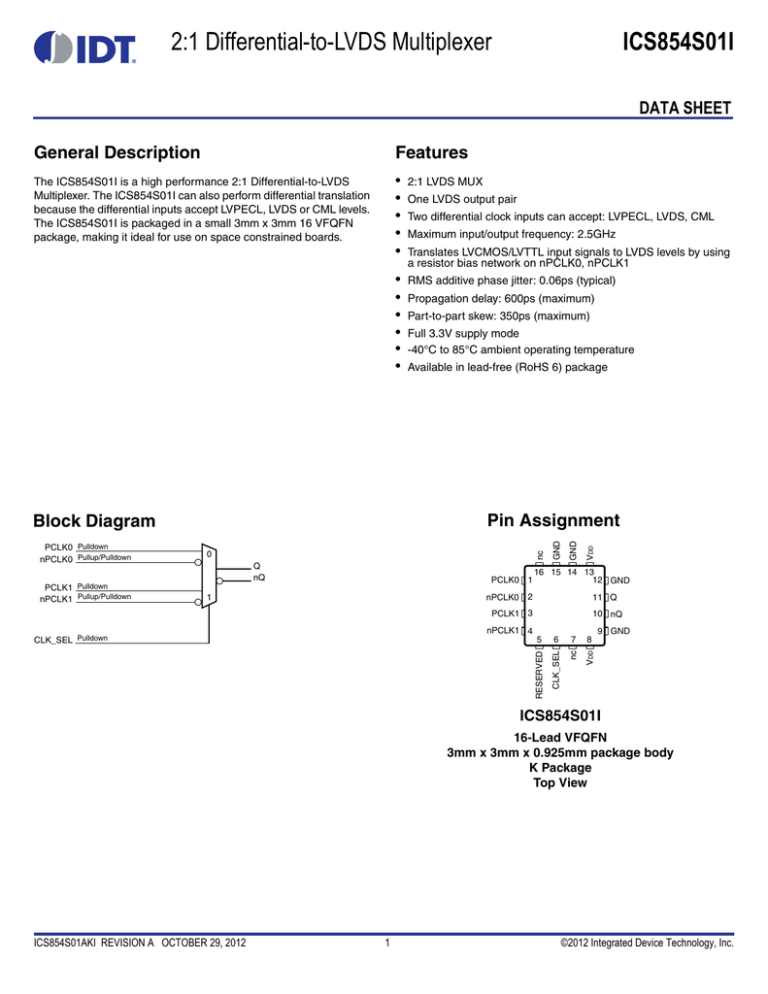
The ICS854S01I is a high performance 2:1 Differential-to-LVDS
Multiplexer. The ICS854S01I can also perform differential translation
because the differential inputs accept LVPECL, LVDS or CML levels.
The ICS854S01I is packaged in a small 3mm x 3mm 16 VFQFN
package, making it ideal for use on space constrained boards.
•
•
•
•
•
2:1 LVDS MUX
•
•
•
•
•
•
RMS additive phase jitter: 0.06ps (typical)
PCLK1 Pulldown
nPCLK1 Pullup/Pulldown
Two differential clock inputs can accept: LVPECL, LVDS, CML
Maximum input/output frequency: 2.5GHz
Translates LVCMOS/LVTTL input signals to LVDS levels by using
a resistor bias network on nPCLK0, nPCLK1
Propagation delay: 600ps (maximum)
Part-to-part skew: 350ps (maximum)
Full 3.3V supply mode
-40°C to 85°C ambient operating temperature
Available in lead-free (RoHS 6) package
Q
nQ
PCLK0 1
nPCLK0
1
VDD
GND
nc
0
GND
Pin Assignment
Block Diagram
PCLK0 Pulldown
nPCLK0 Pullup/Pulldown
One LVDS output pair
16 15 14 13
12 GND
2
11 Q
PCLK1 3
10 nQ
nPCLK1 4
7
8
nc
VDD
6
CLK_SEL
9 GND
5
RESERVED
CLK_SEL Pulldown
ICS854S01I
16-Lead VFQFN
3mm x 3mm x 0.925mm package body
K Package
Top View
ICS854S01AKI REVISION A OCTOBER 29, 2012
1
©2012 Integrated Device Technology, Inc.
ICS854S01I Data Sheet
2:1 DIFFERENTIAL-TO-LVDS MULTIPLEXER
Table 1. Pin Descriptions
Number
Name
1
PCLK0
Input
Type
Pulldown
Non-inverting differential clock input.
Description
2
nPCLK0
Input
Pullup/
Pulldown
Inverting differential clock input. VDD/2 default when left floating.
3
PCLK1
Input
Pulldown
Non-inverting differential clock input.
4
nPCLK1
Input
Pullup/
Pulldown
Inverting differential clock input. VDD/2 default when left floating.
5
RESERVED
Reserve
6
CLK_SEL
Input
7, 16
nc
Unused
Reserve pin.
Pulldown
Clock select input. When HIGH, selects PCLK1, nPCLK1 inputs. When
LOW, selects PCLK0, nPCLK0 inputs. LVCMOS / LVTTL interface levels.
No connects.
8, 13
VDD
Power
Power supply pins.
9, 12, 14, 15
GND
Power
Power supply ground.
10, 11
nQ, Q
Output
Differential output pair. LVDS interface levels.
NOTE: Pullup and Pulldown refer to internal input resistors. See Table 2, Pin Characteristics, for typical values.
Table 2. Pin Characteristics
Symbol
Parameter
Test Conditions
Minimum
Typical
Maximum
Units
CIN
Input Capacitance
2
pF
RPULLUP
Input Pullup Resistor
37
k
RPULLDOWN
Input Pulldown Resistor
37
k
Function Tables
Table 3. Control Input Function Table
CLK_SEL
PCLK Selected
0
PCLK0, nPCLK0
1
PCLK1, nPCLK1
ICS854S01AKI REVISION A OCTOBER 29, 2012
2
©2012 Integrated Device Technology, Inc.
ICS854S01I Data Sheet
2:1 DIFFERENTIAL-TO-LVDS MULTIPLEXER
Absolute Maximum Ratings
NOTE: Stresses beyond those listed under Absolute Maximum Ratings may cause permanent damage to the device.
These ratings are stress specifications only. Functional operation of product at these conditions or any conditions beyond
those listed in the DC Characteristics or AC Characteristics is not implied. Exposure to absolute maximum rating conditions for
extended periods may affect product reliability.
Item
Rating
Supply Voltage, VDD
4.6V
Inputs, VI
-0.5V to VDD + 0.5V
Outputs, IO
Continuous Current
Surge Current
10mA
15mA
Package Thermal Impedance, JA
74.7C/W (0 mps)
Storage Temperature, TSTG
-65C to 150C
DC Electrical Characteristics
Table 4A. Power Supply DC Characteristics, VDD = 3.3V ± 5%, TA = -40°C to 85°C
Symbol
Parameter
Test Conditions
VDD
Power Supply Voltage
IDD
Power Supply Current
Minimum
Typical
Maximum
Units
3.135
3.3
3.465
V
40
mA
Maximum
Units
Table 4B. LVCMOS/LVTTL DC Characteristics, VDD = 3.3V ± 5%, TA = -40°C to 85°C
Symbol
Parameter
Test Conditions
Minimum
Typical
VIH
Input High Voltage
2.2
VDD + 0.3
V
VIL
Input Low Voltage
-0.3
0.8
V
IIH
Input High Current
CLK_SEL
VDD = VIN = 3.465V
150
µA
IIL
Input Low Current
CLK_SEL
VDD = 3.465V, VIN = 0V
-10
µA
Table 4C. LVPECL DC Characteristics, VDD = 3.3V ± 5%, TA = -40°C to 85°C
Symbol
Parameter
Test Conditions
Minimum
IIH
Input High
Current
PCLK0, nPCLK0,
PCLK1, nPCLK1
Input Low
Current
PCLK0, PCLK1
VDD = 3.465V, VIN = 0V
-10
µA
IIL
nPCLK0, nPCLK1
VDD = 3.465V, VIN = 0V
-150
µA
VPP
Peak-to-Peak Voltage; NOTE 1
0.15
1.2
V
VCMR
Common Mode Input Voltage;
NOTE 1, 2
1.2
VDD
V
VDD = VIN = 3.465V
Typical
Maximum
Units
150
µA
NOTE 1: VIL should not be less than -0.3V.
NOTE 2: Common mode input voltage is defined as VIH.
ICS854S01AKI REVISION A OCTOBER 29, 2012
3
©2012 Integrated Device Technology, Inc.
ICS854S01I Data Sheet
2:1 DIFFERENTIAL-TO-LVDS MULTIPLEXER
Table 4D. LVDS DC Characteristics, VDD = 3.3V ± 5%, TA = -40°C to 85°C
Symbol
Parameter
VOD
Differential Output Voltage
VOD
VOD Magnitude Change
VOS
Offset Voltage
VOS
VOS Magnitude Change
Test Conditions
Minimum
Typical
247
1.125
Maximum
Units
454
mV
50
mV
1.375
V
50
mV
Maximum
Units
2.5
GHz
600
ps
AC Electrical Characteristics
Table 5. AC Characteristics, VDD = 3.3V ± 5%, TA = -40°C to 85°C
Symbol
Parameter
fOUT
Output Frequency
tPD
Propagation Delay;
NOTE 1
tjit
Buffer Additive Phase Jitter,
RMS; refer to Additive Phase
Jitter Section
tsk(pp)
Part-to-Part Skew;
NOTE 2, 3
tR / tF
Output Rise/Fall Time
odc
Output Duty Cycle
MUX_ISOLATION
MUX Isolation;
NOTE 4
Test Conditions
Minimum
250
155.52MHz, Integration Range:
12kHz – 20MHz)
20% to 80%
fOUT = 155.52MHz, VPP =
400mV
Typical
400
0.06
ps
350
ps
100
275
ps
49
51
%
86
dB
NOTE: Electrical parameters are guaranteed over the specified ambient operating temperature range, which is established when the device is
mounted in a test socket with maintained transverse airflow greater than 500 lfpm. The device will meet specifications after thermal equilibrium
has been reached under these conditions.
NOTE: All parameters measured at 1.0GHz unless otherwise noted.
NOTE 1: Measured from the differential input crossing point to the differential output crossing point.
NOTE 2: Defined as skew between outputs on different devices operating at the same supply voltage, same temperature, same frequency and
with equal load conditions. Using the same type of inputs on each device, the outputs are measured
at the differential cross points.
NOTE 3: This parameter is defined in accordance with JEDEC Standard 65.
NOTE 4: Q, nQ outputs measured differentially. See Parameter Measurement Information to MUX Isolation diagram.
ICS854S01AKI REVISION A OCTOBER 29, 2012
4
©2012 Integrated Device Technology, Inc.
ICS854S01I Data Sheet
2:1 DIFFERENTIAL-TO-LVDS MULTIPLEXER
Additive Phase Jitter
The spectral purity in a band at a specific offset from the fundamental
compared to the power of the fundamental is called the dBc Phase
Noise. This value is normally expressed using a Phase noise plot
and is most often the specified plot in many applications. Phase noise
is defined as the ratio of the noise power present in a 1Hz band at a
specified offset from the fundamental frequency to the power value of
the fundamental. This ratio is expressed in decibels (dBm) or a ratio
of the power in the 1Hz band to the power in the fundamental. When
the required offset is specified, the phase noise is called a dBc value,
which simply means dBm at a specified offset from the fundamental.
By investigating jitter in the frequency domain, we get a better
understanding of its effects on the desired application over the entire
time record of the signal. It is mathematically possible to calculate an
expected bit error rate given a phase noise plot.
SSB Phase Noise dBc/Hz
Additive Phase Jitter @ 155.52MHz
12kHz to 20MHz = 0.06ps (typical)
Offset from Carrier Frequency (Hz)
As with most timing specifications, phase noise measurements has
issues relating to the limitations of the equipment. Often the noise
floor of the equipment is higher than the noise floor of the device. This
is illustrated above. The device meets the noise floor of what is
shown, but can actually be lower. The phase noise is dependent on
the input source and measurement equipment.
ICS854S01AKI REVISION A OCTOBER 29, 2012
The source generator "IFR2042 10kHz – 56.4GHz Low Noise Signal
Generator as external input to an Agilent 8133A 3GHz Pulse
Generator"
5
©2012 Integrated Device Technology, Inc.
ICS854S01I Data Sheet
2:1 DIFFERENTIAL-TO-LVDS MULTIPLEXER
Parameter Measurement Information
VDD
SCOPE
3.3V±5%
POWER SUPPLY
+ Float GND –
Q
VDD
nPCLK[0:1]
V
Cross Points
PP
V
CMR
PCLK[0:1]
nQ
GND
LVDS Output Load AC Test Circuit
Differential Input Level
Spectrum of Output Signal Q
MUX selects active
input clock signal
A0
Par t 1
Amplitude (dB)
nQx
Qx
nQy Par t 2
MUX_ISOL = A0 – A1
MUX selects static input
A1
Qy
tsk(pp)
ƒ
(fundamental)
Part-to-Part Skew
Frequency
MUX Isolation
nPCLK[0:1]
nQ
80%
80%
PCLK[0:1
VOD
Q
nQ
20%
20%
tR
tF
Q
tPD
Output Rise/Fall Time
ICS854S01AKI REVISION A OCTOBER 29, 2012
Propagation Delay
6
©2012 Integrated Device Technology, Inc.
ICS854S01I Data Sheet
2:1 DIFFERENTIAL-TO-LVDS MULTIPLEXER
Parameter Measurement Information, continued
nQ
VDD
Q
out
t PW
t
PERIOD
DC Input
odc =
t PW
LVDS
100
x 100%
out
t PERIOD
Output Duty Cycle/Pulse Width/Period
Differential Output Voltage Setup
VDD
out
DC Input
LVDS
out
VOS/Δ VOS
ä
Offset Voltage Setup
ICS854S01AKI REVISION A OCTOBER 29, 2012
7
©2012 Integrated Device Technology, Inc.
ICS854S01I Data Sheet
2:1 DIFFERENTIAL-TO-LVDS MULTIPLEXER
Application Information
Wiring the Differential Input to Accept Single Ended Levels
Figure 1 shows how the differential input can be wired to accept
single ended levels. The reference voltage V_REF = VDD/2 is
generated by the bias resistors R1, R2 and C1. This bias circuit
should be located as close as possible to the input pin. The ratio of
R1 and R2 might need to be adjusted to position the V_REF in the
center of the input voltage swing. For example, if the input clock swing
is only 2.5V and VDD = 3.3V, V_REF should be 1.25V and R2/R1 =
0.609.
VDD
R1
1K
CLK_IN
PCLKx
V_REF
nPCLKx
C1
0.1uF
R2
1K
Figure 1. Single-Ended Signal Driving Differential Input
Recommendations for Unused Input Pins
Inputs:
PCLK/nPCLK Inputs:
For applications not requiring the use of the differential input, both
PCLK and nPCLK can be left floating. Though not required, but for
additional protection, a 1k resistor can be tied from PCLK to
ground.
ICS854S01AKI REVISION A OCTOBER 29, 2012
8
©2012 Integrated Device Technology, Inc.
ICS854S01I Data Sheet
2:1 DIFFERENTIAL-TO-LVDS MULTIPLEXER
LVPECL Clock Input Interface
The PCLK /nPCLK accepts LVPECL, LVDS and other differential
signals. Both signals must meet the VPP and VCMR input
requirements. Figures 2A to 2C show interface examples for the
PCLK/ nPCLK input driven by the most common driver types. The
input interfaces suggested here are examples only. If the driver is
from another vendor, use their termination recommendation. Please
consult with the vendor of the driver component to confirm the driver
termination requirements.
3.3V
3.3V
3.3V
3.3V
R3
125Ω
3.3V
3.3V
R4
125Ω
R3
84
3.3V LVPECL
Zo = 50Ω
Zo = 50Ω
C1
Zo = 50Ω
C2
R4
84
PCLK
PCLK
Zo = 50Ω
nPCLK
nPCLK
LVPECL
Input
LVPECL
R1
84Ω
R2
84Ω
R5
100 - 200
Figure 2A. PCLK/nPCLK Input Driven by a
3.3V LVDS Driver
R6
100 - 200
R1
125
LVPECL
Input
R2
125
Figure 2B. PCLK/nPCLK Input Driven by a
3.3V LVPECL Driver with AC Couple
3.3V
3.3V
3.3V
R3
125Ω
3.3V
3.3V
R4
125Ω
Zo = 50Ω
Zo = 50Ω
PCLK
PCLK
Zo = 50Ω
R1
100Ω
nPCLK
LVPECL
Input
LVPECL
R1
84Ω
R2
84Ω
nPCLK
Zo = 50Ω
LVPECL
CML Built-In Pullup
Input
Figure 2C. PCLK/nPCLK Input Driven by a
3.3V LVPECL Driver
Figure 2D. PCLK/nPCLK Input Driven by a
Built-In Pullup CML Driver
3.3V
3.3V
3.3V
R1
50Ω
R2
50Ω
Zo = 50Ω
PCLK
Zo = 50Ω
nPCLK
CML
LVPECL
Input
Figure 2E. PCLK/nPCLK Input Driven by a CML Driver
ICS854S01AKI REVISION A OCTOBER 29, 2012
9
©2012 Integrated Device Technology, Inc.
ICS854S01I Data Sheet
2:1 DIFFERENTIAL-TO-LVDS MULTIPLEXER
Application Schematic Example
Figure 3 shows an example of ICS854S01I application schematic.
This device can accept different types of input signal. In this example,
the input is driven by a LVDS driver. The decoupling capacitor should
be located as close as possible to the power pin.
Note: Thermal pad (E-pad) must be connected to ground (GND).
3.3V
C1
0.1u
R2
100
LVDS
nc
GND
GND
VDD
U1
1
2
3
4
PCLK0
nPCLK0
PCLK1
nPCLK1
ICS854S01i
R3
100
5
6
7
8
3.3V
RESERVED
CLK_SEL
nc
VDD
Zo_diff = 100 Ohm
16
15
14
13
3.3V
R4
1K
GND
Q
nQ
GND
12
11
10
9
+
R1
100
-
Zo_diff = 100 Ohm
3.3V
C2
0.1u
LVDS
Zo_diff = 100 Ohm
Figure 3. ICS854S01I Application Schematic Example
ICS854S01AKI REVISION A OCTOBER 29, 2012
10
©2012 Integrated Device Technology, Inc.
ICS854S01I Data Sheet
2:1 DIFFERENTIAL-TO-LVDS MULTIPLEXER
VFQFN EPAD Thermal Release Path
In order to maximize both the removal of heat from the package and
the electrical performance, a land pattern must be incorporated on
the Printed Circuit Board (PCB) within the footprint of the package
corresponding to the exposed metal pad or exposed heat slug on the
package, as shown in Figure 4. The solderable area on the PCB, as
defined by the solder mask, should be at least the same size/shape
as the exposed pad/slug area on the package to maximize the
thermal/electrical performance. Sufficient clearance should be
designed on the PCB between the outer edges of the land pattern
and the inner edges of pad pattern for the leads to avoid any shorts.
and dependent upon the package power dissipation as well as
electrical conductivity requirements. Thus, thermal and electrical
analysis and/or testing are recommended to determine the minimum
number needed. Maximum thermal and electrical performance is
achieved when an array of vias is incorporated in the land pattern. It
is recommended to use as many vias connected to ground as
possible. It is also recommended that the via diameter should be 12
to 13mils (0.30 to 0.33mm) with 1oz copper via barrel plating. This is
desirable to avoid any solder wicking inside the via during the
soldering process which may result in voids in solder between the
exposed pad/slug and the thermal land. Precautions should be taken
to eliminate any solder voids between the exposed heat slug and the
land pattern. Note: These recommendations are to be used as a
guideline only. For further information, please refer to the Application
Note on the Surface Mount Assembly of Amkor’s Thermally/
Electrically Enhance Leadframe Base Package, Amkor Technology.
While the land pattern on the PCB provides a means of heat transfer
and electrical grounding from the package to the board through a
solder joint, thermal vias are necessary to effectively conduct from
the surface of the PCB to the ground plane(s). The land pattern must
be connected to ground through these vias. The vias act as “heat
pipes”. The number of vias (i.e. “heat pipes”) are application specific
PIN
PIN PAD
SOLDER
EXPOSED HEAT SLUG
GROUND PLANE
THERMAL VIA
SOLDER
LAND PATTERN
(GROUND PAD)
PIN
PIN PAD
Figure 4. P.C. Assembly for Exposed Pad Thermal Release Path – Side View (drawing not to scale)
ICS854S01AKI REVISION A OCTOBER 29, 2012
11
©2012 Integrated Device Technology, Inc.
ICS854S01I Data Sheet
2:1 DIFFERENTIAL-TO-LVDS MULTIPLEXER
3.3V LVDS Driver Termination
A general LVDS interface is shown in Figure 5 In a 100 differential
transmission line environment, LVDS drivers require a matched load
termination of 100 across near the receiver input. For a multiple
LVDS outputs buffer, if only partial outputs are used, it is
recommended to terminate the unused outputs.
3.3V
50Ω
3.3V
LVDS Driver
+
R1
100Ω
–
50Ω
100Ω Differential Transmission Line
Figure 5. Typical LVDS Driver Termination
ICS854S01AKI REVISION A OCTOBER 29, 2012
12
©2012 Integrated Device Technology, Inc.
ICS854S01I Data Sheet
2:1 DIFFERENTIAL-TO-LVDS MULTIPLEXER
Power Considerations
This section provides information on power dissipation and junction temperature for the ICS854S01I.
Equations and example calculations are also provided.
1.
Power Dissipation.
The total power dissipation for theICS854S01I is the sum of the core power plus the power dissipated in the load(s).
The following is the power dissipation for VDD = 3.3V + 5% = 3.465V, which gives worst case results.
NOTE: Please refer to Section 3 for details on calculating power dissipated in the load.
•
Power (core)MAX = VDD_MAX * IDD_MAX = 3.465V * 40mA = 138.6mW
2. Junction Temperature.
Junction temperature, Tj, is the temperature at the junction of the bond wire and bond pad directly affects the reliability of the device. The
maximum recommended junction temperature is 125°C. Limiting the internal transistor junction temperature, Tj, to 125°C ensures that the bond
wire and bond pad temperature remains below 125°C.
The equation for Tj is as follows: Tj = JA * Pd_total + TA
Tj = Junction Temperature
JA = Junction-to-Ambient Thermal Resistance
Pd_total = Total Device Power Dissipation (example calculation is in section 1 above)
TA = Ambient Temperature
In order to calculate junction temperature, the appropriate junction-to-ambient thermal resistance JA must be used. Assuming no air flow and
a multi-layer board, the appropriate value is 74.7°C/W per Table 6 below.
Therefore, Tj for an ambient temperature of 85°C with all outputs switching is:
85°C + 0.139W * 74.7°C/W = 95.4°C. This is well below the limit of 125°C.
This calculation is only an example. Tj will obviously vary depending on the number of loaded outputs, supply voltage, air flow and the type of
board (multi-layer).
Table 6. Thermal Resistance JA for 16 Lead VFQFN, Forced Convection
JA by Velocity
Meters per Second
Multi-Layer PCB, JEDEC Standard Test Boards
ICS854S01AKI REVISION A OCTOBER 29, 2012
0
1
2.5
74.7°C/W
65.3°C/W
58.5°C/W
13
©2012 Integrated Device Technology, Inc.
ICS854S01I Data Sheet
2:1 DIFFERENTIAL-TO-LVDS MULTIPLEXER
Reliability Information
Table 7. JA vs. Air Flow Table for a 16 Lead VFQFN
JA by Velocity
Meters per Second
Multi-Layer PCB, JEDEC Standard Test Boards
0
1
2.5
74.7°C/W
65.3°C/W
58.5°C/W
Transistor Count
The transistor count for ICS854S01I is: 257
This is a suggested replacement for ICS85401
ICS854S01AKI REVISION A OCTOBER 29, 2012
14
©2012 Integrated Device Technology, Inc.
ICS854S01I Data Sheet
2:1 DIFFERENTIAL-TO-LVDS MULTIPLEXER
Package Outline and Package Dimensions
Package Outline - K Suffix for 16 Lead VFQFN
Seating Plane
(R ef.)
A1
Index Area
A3
N
Anvil
Singulation
or
Sawn
Singulation
Top View
(Ref.)
ND & NE
Even
(ND-1)x e
L
N
e (Typ.)
2 If ND & NE
1
are Even
2
E2
(NE -1)x e
(Re f.)
E2
2
b
A
D
0. 08
Chamfer 4x
0.6 x 0.6 max
OPTIONAL
(Ref.)
e
ND & NE
Odd
C
Thermal
Base
D2
2
D2
C
Bottom View w/Type A ID
Bottom View w/Type C ID
2
1
2
1
CHAMFER
4
RADIUS
N N-1
4
N N-1
There are 2 methods of indicating pin 1 corner at the back of the VFQFN package are:
1. Type A: Chamfer on the paddle (near pin 1)
2. Type C: Mouse bite on the paddle (near pin 1)
Table 8. Package Dimensions
JEDEC Variation: VEED-2/-4
All Dimensions in Millimeters
Symbol
Minimum
Maximum
N
16
A
0.80
1.00
A1
0
0.05
A3
0.25 Ref.
b
0.18
0.30
4
ND & NE
D&E
3.00 Basic
D2 & E2
1.00
1.80
e
0.50 Basic
L
0.30
0.50
Reference Document: JEDEC Publication 95, MO-220
ICS854S01AKI REVISION A OCTOBER 29, 2012
15
©2012 Integrated Device Technology, Inc.
ICS854S01I Data Sheet
2:1 DIFFERENTIAL-TO-LVDS MULTIPLEXER
Ordering Information
Table 9. Ordering Information
Part/Order Number
854S01AKILF
854S01AKILFT
Marking
4S1A
4S1A
Package
“Lead-Free” 16 Lead VFQFN
“Lead-Free” 16 Lead VFQFN
Shipping Packaging
Tube
Tape & Reel
Temperature
-40C to 85C
-40C to 85C
NOTE: Parts that are ordered with an "LF" suffix to the part number are the Pb-Free configuration and are RoHS compliant.
ICS854S01AKI REVISION A OCTOBER 29, 2012
16
©2012 Integrated Device Technology, Inc.
ICS854S01I Data Sheet
2:1 DIFFERENTIAL-TO-LVDS MULTIPLEXER
Revision History Sheet
Rev
Table
Page
1
A
T9
A
Description of Change
Date
9
16
Deleted HiperClockS Logo. Updated GD paragraph to include CML.
Added CML to 3rd bullet.
Added figures 2D and 2E.
Deleted quantity from tape and reel.
10/29/12
10
Added Note: Thermal pad (E-pad) must be connected to ground (GND).
11/2/12
ICS854S01AKI REVISION A OCTOBER 29, 2012
17
©2012 Integrated Device Technology, Inc.
ICS854S01I Data Sheet
2:1 DIFFERENTIAL-TO-LVDS MULTIPLEXER
We’ve Got Your Timing Solution
6024 Silver Creek Valley Road
San Jose, California 95138
Sales
800-345-7015 (inside USA)
+408-284-8200 (outside USA)
Fax: 408-284-2775
www.IDT.com/go/contactIDT
Technical Support
netcom@idt.com
+480-763-2056
DISCLAIMER Integrated Device Technology, Inc. (IDT) and its subsidiaries reserve the right to modify the products and/or specifications described herein at any time and at IDT’s sole discretion. All information in this document,
including descriptions of product features and performance, is subject to change without notice. Performance specifications and the operating parameters of the described products are determined in the independent state and are not
guaranteed to perform the same way when installed in customer products. The information contained herein is provided without representation or warranty of any kind, whether express or implied, including, but not limited to, the
suitability of IDT’s products for any particular purpose, an implied warranty of merchantability, or non-infringement of the intellectual property rights of others. This document is presented only as a guide and does not convey any
license under intellectual property rights of IDT or any third parties.
IDT’s products are not intended for use in applications involving extreme environmental conditions or in life support systems or similar devices where the failure or malfunction of an IDT product can be reasonably expected to significantly affect the health or safety of users. Anyone using an IDT product in such a manner does so at their own risk, absent an express, written agreement by IDT.
Integrated Device Technology, IDT and the IDT logo are registered trademarks of IDT. Other trademarks and service marks used herein, including protected names, logos and designs, are the property of IDT or their respective third
party owners.
Copyright 2012. All rights reserved.


