AD8346 Evaluation Board
EVAL-AD8346EB
BOARD DESCRIPTION
The AD8346 evaluation board has been carefully laid out and
tested to demonstrate the specified high speed performance of
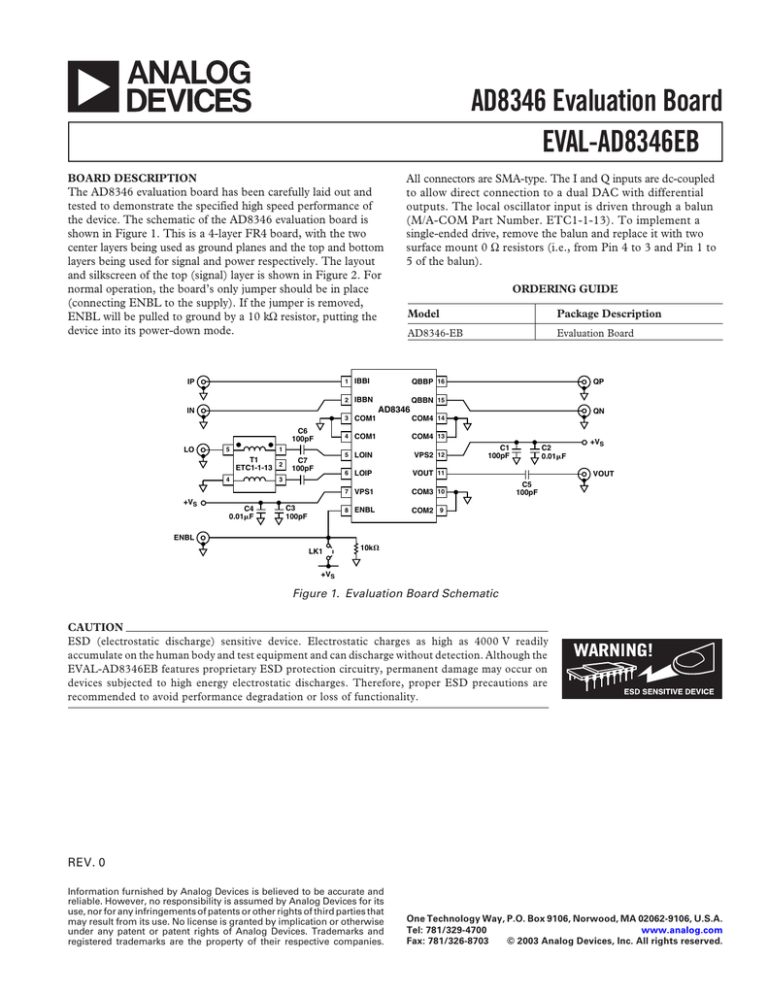
the device. The schematic of the AD8346 evaluation board is
shown in Figure 1. This is a 4-layer FR4 board, with the two
center layers being used as ground planes and the top and bottom
layers being used for signal and power respectively. The layout
and silkscreen of the top (signal) layer is shown in Figure 2. For
normal operation, the board’s only jumper should be in place
(connecting ENBL to the supply). If the jumper is removed,
ENBL will be pulled to ground by a 10 kW resistor, putting the
device into its power-down mode.
All connectors are SMA-type. The I and Q inputs are dc-coupled
to allow direct connection to a dual DAC with differential
outputs. The local oscillator input is driven through a balun
(M/A-COM Part Number. ETC1-1-13). To implement a
single-ended drive, remove the balun and replace it with two
surface mount 0 W resistors (i.e., from Pin 4 to 3 and Pin 1 to
5 of the balun).
ORDERING GUIDE
Model
Package Description
AD8346-EB
Evaluation Board
1 IBBI
IP
2 IBBN
C6
100pF
5
1
T1
2
ETC1-1-13
4
+VS
QBBN 15
AD8346
IN
LO
QP
QBBP 16
C4
0.01F
C7
100pF
3
C3
100pF
QN
3 COM1
COM4 14
4 COM1
COM4 13
5 LOIN
VPS2 12
6 LOIP
VOUT 11
7 VPS1
COM3 10
8 ENBL
COM2 9
C1
100pF
C2
0.01F
+VS
VOUT
C5
100pF
ENBL
LK1
10k⍀
+VS
Figure 1. Evaluation Board Schematic
CAUTION
ESD (electrostatic discharge) sensitive device. Electrostatic charges as high as 4000 V readily
accumulate on the human body and test equipment and can discharge without detection. Although the
EVAL-AD8346EB features proprietary ESD protection circuitry, permanent damage may occur on
devices subjected to high energy electrostatic discharges. Therefore, proper ESD precautions are
recommended to avoid performance degradation or loss of functionality.
REV. 0
Information furnished by Analog Devices is believed to be accurate and
reliable. However, no responsibility is assumed by Analog Devices for its
use, nor for any infringements of patents or other rights of third parties that
may result from its use. No license is granted by implication or otherwise
under any patent or patent rights of Analog Devices. Trademarks and
registered trademarks are the property of their respective companies.
One Technology Way, P.O. Box 9106, Norwood, MA 02062-9106, U.S.A.
Tel: 781/329-4700
www.analog.com
Fax: 781/326-8703
© 2003 Analog Devices, Inc. All rights reserved.
C03314–0–1/03(0)
EVAL-AD8346EB
PRINTED IN U.S.A.
Figure 2. Layout and Silkscreen of Evaluation Board Signal Layer
–2–
REV. 0

