NI PCI-6110/6111 Specifications
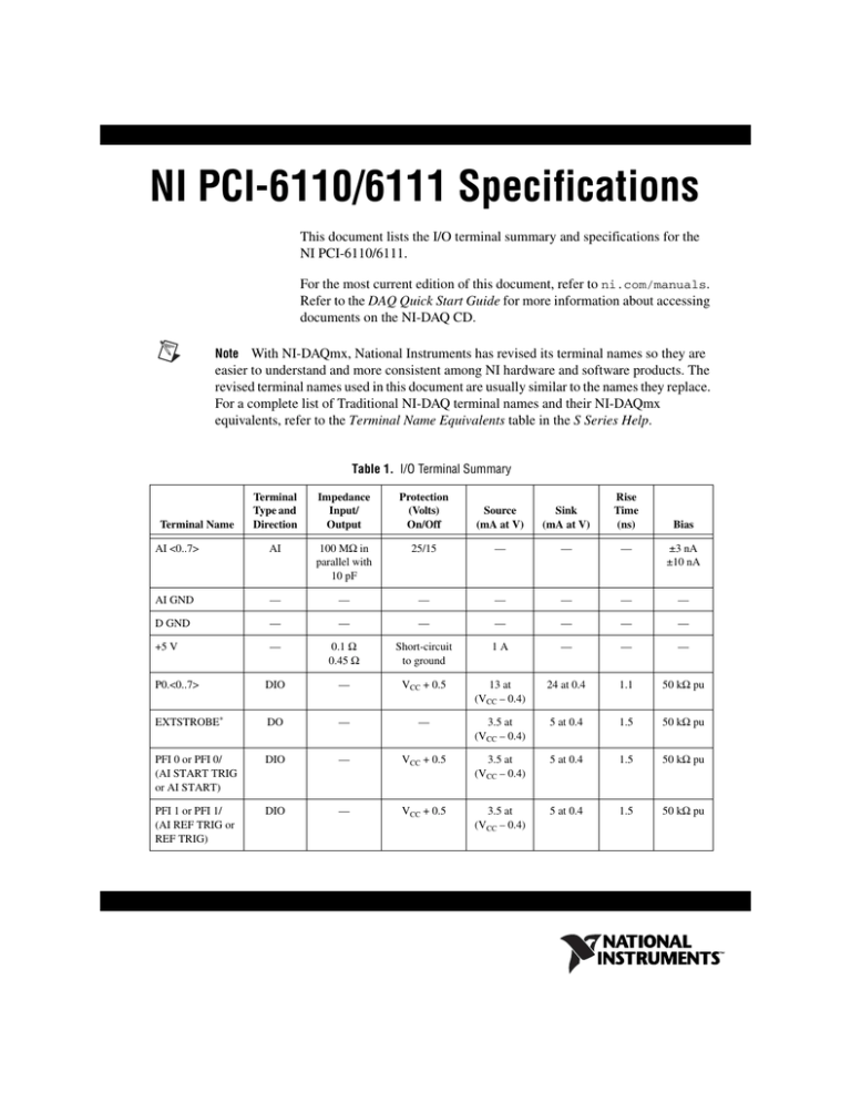
This document lists the I/O terminal summary and specifications for the
NI PCI-6110/6111.
For the most current edition of this document, refer to ni.com/manuals.
Refer to the DAQ Quick Start Guide for more information about accessing
documents on the NI-DAQ CD.
With NI-DAQmx, National Instruments has revised its terminal names so they are
easier to understand and more consistent among NI hardware and software products. The
revised terminal names used in this document are usually similar to the names they replace.
For a complete list of Traditional NI-DAQ terminal names and their NI-DAQmx
equivalents, refer to the Terminal Name Equivalents table in the S Series Help.
Note
Table 1. I/O Terminal Summary
Terminal
Type and
Direction
Impedance
Input/
Output
Protection
(Volts)
On/Off
Source
(mA at V)
Sink
(mA at V)
Rise
Time
(ns)
AI <0..7>
AI
100 MΩ in
parallel with
10 pF
25/15
—
—
—
±3 nA
±10 nA
AI GND
—
—
—
—
—
—
—
D GND
—
—
—
—
—
—
—
+5 V
—
0.1 Ω
0.45 Ω
Short-circuit
to ground
1A
—
—
—
P0.<0..7>
DIO
—
VCC + 0.5
13 at
(VCC – 0.4)
24 at 0.4
1.1
50 kΩ pu
EXTSTROBE*
DO
—
—
3.5 at
(VCC – 0.4)
5 at 0.4
1.5
50 kΩ pu
PFI 0 or PFI 0/
(AI START TRIG
or AI START)
DIO
—
VCC + 0.5
3.5 at
(VCC – 0.4)
5 at 0.4
1.5
50 kΩ pu
PFI 1 or PFI 1/
(AI REF TRIG or
REF TRIG)
DIO
—
VCC + 0.5
3.5 at
(VCC – 0.4)
5 at 0.4
1.5
50 kΩ pu
Terminal Name
Bias
Table 1. I/O Terminal Summary (Continued)
Terminal
Type and
Direction
Impedance
Input/
Output
Protection
(Volts)
On/Off
Source
(mA at V)
Sink
(mA at V)
Rise
Time
(ns)
Bias
PFI 2
DIO
—
VCC + 0.5
3.5 at
(VCC – 0.4)
5 at 0.4
1.5
50 kΩ pu
PFI 3 or PFI 3/
(CTR 1 SOURCE
or CTR 1 SRC)
DIO
—
VCC + 0.5
3.5 at
(VCC – 0.4)
5 at 0.4
1.5
50 kΩ pu
PFI 4 or PFI 4/
CTR 1 GATE
DIO
—
VCC + 0.5
3.5 at
(VCC – 0.4)
5 at 0.4
1.5
50 kΩ pu
CTR 1 OUT
DO
—
—
3.5 at
(VCC – 0.4)
5 at 0.4
1.5
50 kΩ pu
PFI 5 or PFI 5/
(AO SAMP CLK
or AO SAMP)
DIO
—
VCC + 0.5
3.5 at
(VCC – 0.4)
5 at 0.4
1.5
50 kΩ pu
PFI 6 or PFI 6/
(AO START TRIG
or AO START)
DIO
—
VCC + 0.5
3.5 at
(VCC – 0.4)
5 at 0.4
1.5
50 kΩ pu
PFI 7 or PFI 7/
(AI SAMP CLK
or AI SAMP)
DIO
—
VCC + 0.5
3.5 at
(VCC – 0.4)
5 at 0.4
1.5
50 kΩ pu
PFI 8 or PFI 8/
(CTR 0 SOURCE
or CTR 0 SRC)
DIO
—
VCC + 0.5
3.5 at
(VCC – 0.4)
5 at 0.4
1.5
50 kΩ pu
PFI 9 or PFI 9/
CTR 0 GATE
DIO
—
VCC + 0.5
3.5 at
(VCC – 0.4)
5 at 0.4
1.5
50 kΩ pu
CTR 0 OUT
DO
—
—
3.5 at
(VCC – 0.4)
5 at 0.4
1.5
50 kΩ pu
FREQ OUT
or F OUT
DO
—
—
3.5 at
(VCC – 0.4)
5 at 0.4
1.5
50 kΩ pu
Terminal Name
*
Indicates active low
AI = Analog Input
AO = Analog Output
DIO = Digital Input/Output
DO = Digital Output
pu = pull-up
Note: The tolerance on the 50 kΩ pull-up resistors is large. Actual value might range between 17 kΩ and 100 kΩ.
NI PCI-6110/6111 Specifications
2
ni.com
Specifications
The following specifications are typical at 25 °C unless otherwise noted.
Analog Input
Input Characteristics
Number of channels
NI PCI-6110.................................... 4 pseudodifferential
NI PCI-6111.................................... 2 pseudodifferential
Type of ADC
Resolution ....................................... 12 bits, 1 in 4,096
Pipeline ........................................... 3
Sampling rate
Maximum........................................ 5 MS/s
Minimum ........................................ 1 kS/s
Input coupling ........................................ DC or AC
Maximum working voltage for all AI channels
Input Channels
AI <0..3>+
Maximum Working Voltage
(Signal + Common Mode)
Range
20 mV to 10 V
Should remain within ±11 V of ground
20 to 42 V
Should remain within ± 42 V of ground
All
Should remain within ±11 V of ground
AI <0..3>–
Overvoltage protection........................... ± 42 V
Inputs protected
Positive input .................................. All channels
Negative input................................. All channels
FIFO buffer size ..................................... 8,192 samples
Data transfers ......................................... DMA, interrupts,
programmed I/O
DMA modes........................................... Scatter-gather (single transfer,
demand transfer)
© National Instruments Corporation
3
NI PCI-6110/6111 Specifications
Accuracy Information
Table 2. NI 6110/6111 Analog Input DC Accuracy Information
Absolute Accuracy
Full
Scale
Nominal
Range
(V)
24 Hours
90 Days
± 42
0.51
± 20
Relative Accuracy
Noise + Quantization
(mV)
% of Reading
Averaged
Temp
Drift
(%/°C)
Theoretical
Averaged
51
4.4
0.0005
24
5.8
20
20
1.8
0.0005
9.8
2.3
0.11
5.7
10
0.88
0.0005
4.9
1.2
0.058
0.059
3
5.1
0.44
0.0005
2.4
0.58
0.057
0.058
0.059
1.3
2
0.18
0.0005
0.98
0.23
±1
0.057
0.058
0.059
0.7
1
0.088
0.0005
0.49
0.12
± 0.5
0.057
0.058
0.059
0.4
0.67
0.059
0.0005
0.24
0.077
± 0.2
0.057
0.058
0.059
0.2
0.39
0.035
0.0005
0.098
0.046
1 Year
Offset
(mV)
Single Pt.
0.51
0.51
35
0.51
0.51
0.51
±10
0.11
0.11
±5
0.057
±2
Resolution (mV)
Note: Accuracies are valid for measurements following an internal calibration.
Measurement accuracies are listed for operational temperatures within ±1 °C of internal calibration temperature and ±10 °C of external or
factory calibration temperature. A one-year calibration interval is recommended.
Transfer Characteristics
INL.......................................................... ± 0.5 LSB typ, ±1 LSB max
DNL ........................................................ ± 0.3 LSB typ, ± 0.75 LSB max
Spurious free dynamic range (SFDR) ....Refer to Table 3
Effective number of bits (ENOB)...........11.0 bits, DC to 100 kHz
Amplifier Characteristics
Input impedance
AI <0..3>+ to AI <0..3>–
Normal powered on..................1 MΩ in parallel with 100 pF
Powered off ..............................1 MΩ minimum
Overload ...................................1 MΩ
Impedance to ground
AI <0..3>– to ground ...............100 GΩ in parallel with 10 nF
Input bias current .................................... ± 300 pA
Input offset current ................................. ± 200 pA
NI PCI-6110/6111 Specifications
4
ni.com
Dynamic Characteristics
Crosstalk................................................. –80 dB, DC to 100 kHz
Table 3. Analog Input Characteristics
Input Range
Bandwidth1
(MHz)
SFDR Typ2
(dB)
SFDR Max
(dB)
CMRR3
(dB)
System
Noise4
(LSBrms)
± 42 V
5.5
78
70
34
0.5
± 20 V
4.4
78
70
40
0.5
± 10 V
7.2
81
75
46
0.5
±5V
4.8
81
75
52
0.5
±2 V
4.8
85
75
60
0.5
±1 V
4.4
85
75
66
0.5
± 500 mV
4.4
85
75
70
0.6
± 200 mV
4.1
81
70
72
1.0
1
–3 dB frequency for input amplitude at 96% of the input range (–0.3 dB)
2
Measured at 100 kHz
3
DC to 60 Hz
4
LSBrms, not including quantization
Bandwidth specifications are for signals on the (+) input with the (–) input at
DC ground. The (–) input is slew rate limited to 24 V/µs and has an additional 10 nF
capacitance to ground.
Note
Stability
Recommended warm-up time ................ 15 minutes
Calibration interval ................................ 1 year
Offset temperature coefficient
Pregain ............................................ ± 5 µV/°C
Postgain........................................... ± 50 µV/°C
Gain temperature coefficient.................. ± 20 ppm/°C
© National Instruments Corporation
5
NI PCI-6110/6111 Specifications
Onboard calibration reference
Level ................................................5.000 V (± 2.5 mV)
(actual value stored in EEPROM)
Temperature coefficient................... ± 2.0 ppm/°C max
Long-term stability .......................... ± 6 ppm/ 1,000 h
Analog Output
Output Characteristics
Number of channels................................2 voltage
Resolution ...............................................16 bits, 1 in 65,536
Max update rate
1 channel..........................................4 MS/s, system dependent
2 channel..........................................2.5 MS/s, system dependent
FIFO buffer size......................................2,048 samples
Data transfers ..........................................DMA, interrupts,
programmed I/O
DMA modes ...........................................Scatter-gather (single transfer,
demand transfer)
Transfer Characteristics
Relative accuracy (INL) ......................... ± 4 LSB typ, ± 8 LSB max
DNL ........................................................ ± 2 LSB typ, ± 8 LSB max
Table 4. NI PCI-6110/6111 Analog Output DC Accuracy Information
Absolute Accuracy
% of Reading
Nominal
Range (V)
24 Hrs
1 Year
Offset
(mV)
Temp Drift
(%/°C)
Absolute Accuracy
at Full Scale (± mV)
±10
0.018
0.022
5.933
0.0005
8.133
Note: Temp Drift applies only if ambient is greater than ±10 °C of previous external calibration.
Voltage Output
Range ...................................................... ±10 V
Output coupling ......................................DC
NI PCI-6110/6111 Specifications
6
ni.com
Output impedance .................................. 50 Ω, ± 5%
Short circuit current ............................... ± 27 mA typ
Current drive .......................................... ± 5 mA min
Output stability....................................... Any passive load
Protection ............................................... Short-circuit to ground
Power-on output voltage ........................ 0, ± 400 mV (before software
loads calibration values)
Dynamic Characteristics
Settling time and slew rate
Settling Time for Full-Scale Step
Slew Rate
300 ns to ±0.01%
300 V/µs
Noise ...................................................... 1 mVrms, DC to 5 MHz
Spurious free dynamic range.................. 75 dB, DC to 10 kHz
Glitch energy.......................................... ± 30 mV for 1 µs
Stability
Offset temperature coefficient ............... ± 500 µV/°C
Gain temperature coefficient
Internal reference ............................ ± 50 ppm/°C
External reference ........................... ± 25 ppm/°C
Onboard calibration reference
Level ............................................... 5.000 V (± 2.5 mV)
(actual value stored in EEPROM)
Temperature coefficient .................. ± 2.0 ppm/°C max
Long-term stability ......................... ± 6 ppm/ 1,000 h
Digital I/O
Number of channels ............................... 8 input/output
Compatibility ......................................... TTL/CMOS
© National Instruments Corporation
7
NI PCI-6110/6111 Specifications
Digital logic levels
Level
Min
Max
Input low voltage
0.0 V
0.8 V
Input high voltage
2.0 V
5.0 V
Input low current (Vin = 0 V)
—
–320 µA
Input high current (Vin = 5 V)
—
10 µA
Output low voltage (IOL = 24 mA)
—
0.4 V
4.35 V
—
Output high voltage (IOH = –13 mA)
Power-on state ........................................Input (high-impedance)
Data transfers ..........................................Programmed I/O
Timing I/O
Counter/Timers
Number of channels................................2
Resolution ...............................................24 bits
Compatibility ..........................................TTL/CMOS
Digital logic levels
Level
Min
Max
Input low voltage
0V
0.8 V
Input high voltage
2V
5V
Output low voltage (IOL = 5 mA)
—
0.4 V
4.35 V
—
Output high voltage (IOH = –3.5 mA)
Base clocks available..............................20 MHz, 100 kHz
Base clock accuracy................................± 0.01%
Max source frequency.............................20 MHz
Min source pulse duration .....................10 ns, edge-detect mode
Min gate pulse duration .........................10 ns, edge-detect mode
NI PCI-6110/6111 Specifications
8
ni.com
Data transfers ......................................... DMA, interrupts,
programmed I/O
DMA modes........................................... Scatter-gather (single transfer,
demand transfer)
Frequency Scaler
Number of channels ............................... 1
Resolution .............................................. 4 bits, 1 in 16
Compatibility ......................................... TTL/CMOS
Digital logic levels
Level
Min
Max
Input low voltage
0V
0.8 V
Input high voltage
2V
5V
Output low voltage (Iout= 5 mA)
—
0.4 V
4.35 V
—
Output low voltage (Iout = –3.5 mA)
Base clocks available ............................. 10 MHz, 100 kHz
Base clock accuracy ............................... ± 0.01%
Data transfers ......................................... DMA, interrupts,
programmed I/O
Triggers
Analog Trigger
Number of triggers ................................. 1
Purpose
Analog input ................................... Start, reference, and pause trigger,
sample clock
Analog output ................................. Start and pause trigger,
sample clock
General-purpose counter/timers...... Source, gate
Source..................................................... All analog input channels,
external trigger
(PFI 0/ AI START TRIG)
© National Instruments Corporation
9
NI PCI-6110/6111 Specifications
Level
Internal source, AI <0..3> ...............± Full-scale
External source, PFI 0/
AI START TRIG............................. ± 10 V
Slope .......................................................Positive or negative
(software-selectable)
Resolution ...............................................8 bits, 1 in 256
Hysteresis................................................Programmable
Bandwidth (–3 dB)
Internal source, AI <0..3> ...............5 MHz
External source, PFI0/TRIG1..........5 MHz
Digital Trigger
Purpose
Analog input ....................................Start, reference, and pause trigger,
sample clock
Analog output ..................................Start and pause trigger,
sample clock
General-purpose counter/timers ......Source, gate
External sources......................................PFI <0..9>, RTSI <0..6>
Compatibility ..........................................5 V/TTL
Response .................................................Rising or falling edge
Pulse width .............................................10 ns min
External Input for Digital or Analog Trigger
(PFI 0/AI START TRIG)
Output impedance...................................10 kΩ
Source impedance (recommended).........1 kΩ
Coupling .................................................DC or AC
Protection
Digital trigger ..................................–0.5 V to (VCC + 0.5) V
Analog trigger
On/disabled............................... ± 35 V
Powered off .............................. ± 35 V
NI PCI-6110/6111 Specifications
10
ni.com
RTSI
Trigger lines ........................................... 7
Bus Interface
Type ....................................................... Master, slave
Power Requirement
+5 VDC (± 5%)
NI PCI-6110.................................... 2.5 A
NI PCI-6111.................................... 2.0 A
Power available at I/O connector ........... +4.65 to +5.25 VDC at 1 A
Physical
Dimensions
(not including connectors) ..................... 31.2 cm by 10.6 cm
(12.3 in. by 4.2 in.)
I/O connector.......................................... 68-pin male SCSI-II type
Maximum Working Voltage
Maximum working voltage refers to the signal voltage plus the
common-mode voltage.
Channel-to-earth..................................... 42 V, Installation Category I
Channel-to-channel ................................ 42 V, Installation Category I
Environmental
Operating temperature............................ 0 to 45 °C
Storage temperature ............................... –20 to 70 °C
Humidity ................................................ 5 to 90% RH, noncondensing
Maximum altitude .................................. 2,000 m
Pollution Degree (indoor use only) ........ 2
Clean the device with a soft, non-metallic brush. Make sure that the device is
completely dry and free from contaminants before returning it to service.
Note
© National Instruments Corporation
11
NI PCI-6110/6111 Specifications
Safety
This product is designed to meet the requirements of the following
standards of safety for electrical equipment for measurement, control,
and laboratory use:
•
IEC 61010-1, EN 61010-1
•
UL 3111-1, UL 61010B-1
•
CAN/CSA C22.2 No. 1010.1
Note For UL and other safety certifications, refer to the product label, or visit
ni.com/hardref.nsf, search by model number or product line, and click the
appropriate link in the Certification column.
Electromagnetic Compatibility
Emissions................................................EN 55011 Class A at 10 m
FCC Part 15A above 1 GHz
Immunity ................................................EN 61326:1997A2:2001,
Table 1
EMC/EMI ...............................................CE, C-Tick, and FCC Part 15
(Class A) Compliant
Note
For EMC compliance, you must operate this device with shielded cabling.
CE Compliance
This product meets the essential requirements of applicable European
Directives, as amended for CE marking, as follows:
Low-Voltage Directive (safety).............. 73/23/EEC
Electromagnetic Compatibility
Directive (EMC) ..................................... 89/336/EEC
Refer to the Declaration of Conformity (DoC) for this product for any additional
regulatory compliance information. To obtain the DoC for this product, visit
ni.com/hardref.nsf, search by model number or product line, and click the
appropriate link in the Certification column.
Note
National Instruments™, ni.com™, NI™, NI-DAQ™, and RTSI™ are trademarks of National Instruments
Corporation. Product and company names mentioned herein are trademarks or trade names of their
respective companies. For patents covering National Instruments products, refer to the appropriate
location: Help»Patents in your software, the patents.txt file on your CD, or ni.com/patents.
© 2004 National Instruments Corp. All rights reserved.
*370980A-01*
370980A-01
Feb04


