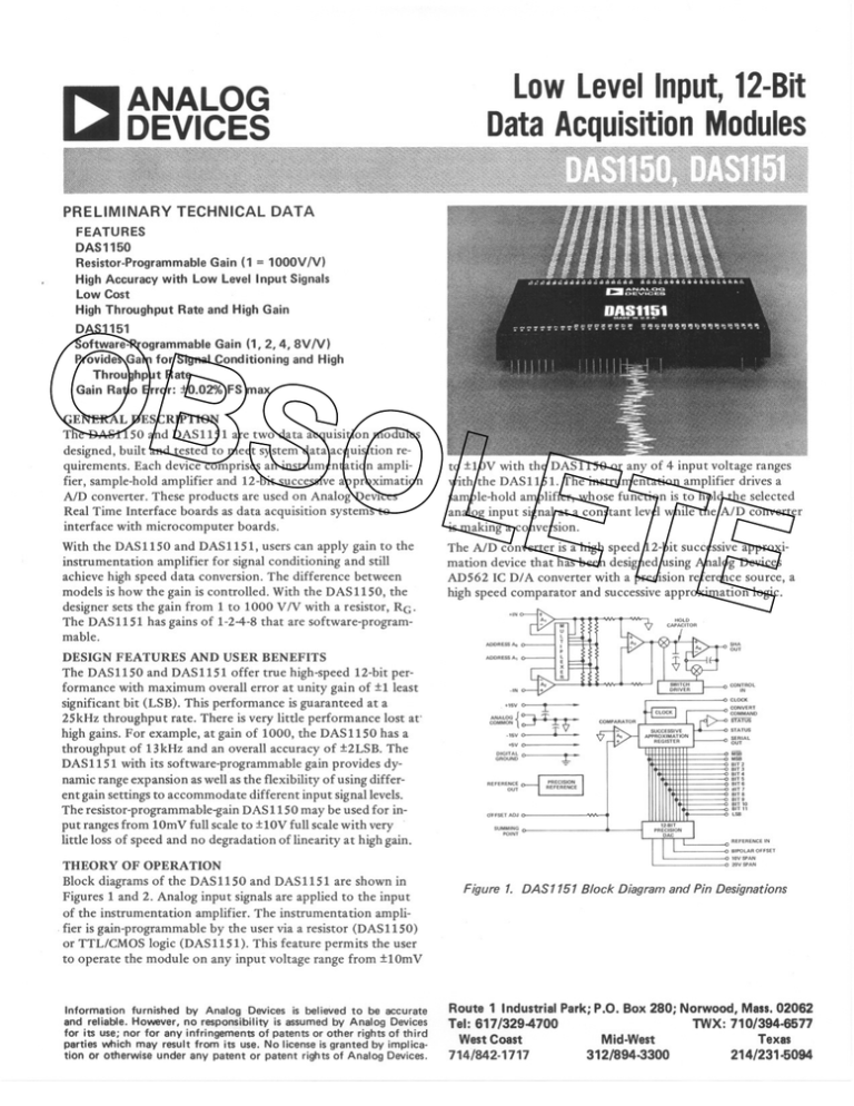
Analog Devices DAS1151 A/D Converter Datasheet
advertisement

LowLevelInput,12-Bit
-.. ANALOG
W DEVICES
DataAcquisition
Modules
PRELIMINARY TECHNICAL DATA
FEATURES
DAS1150
Resistor-Programmable Gain (1 = 1000V!V)
High Accuracy with Low Level Input Signals
Low Cost
High Throughput Rate and High Gain
DAS1151
Software-Programmable Gain (1, 2, 4, 8V!V)
Provides Gain for Signal Conditioning and High
Throughput Rate
Gain Ratio Error: :1:0.02%FS max
OBS
OLE
GENERAL DESCRIPTION
The DAS1150 and DAS1151 are two data acquisition modules
designed, built and tested to meet system data acquisition requirements. Each device comprises an instrumentation amplifier, sample-hold amplifier and 12-bit successive approximation
AID converter. These products are used on Analog Devices
Real Time Interface boards as data acquisition systems to
interface with microcomputer boards.
With the DAS1150 and DAS1151, users can apply gain to the
instrumentation amplifier for signal conditioning and still
achieve high speed data conversion. The difference between
models is how the gain is controlled. With the DAS 1150, the
designer sets the gain from 1 to 1000 V/V with a resistor, RG.
The DAS1151 has gains of 1-2-4-8 that are software-programmable.
DESIGN FEATURES AND USER BENEFITS
The DAS1150 and DAS1151 offer true high-speed 12-bit performancewith maximum overall error at unity gain of :1:1least
significant bit (LSB). This performance is guaranteed at a
25kHz throughput rate. There is very little performance lost at'
high gains. For example, at gain of 1000, the DAS1l50 has a
throughput of 13kHz and an overall accuracy of :l:2LSB. The
DAS1151 with its software-programmable gain provides dynamic range expansion as well as the flexibility of using different gain settings to accommodate different input signal levels.
The resistor-programmable-gain DAS 1150 may be used for input ranges from 1OmV full scale to :l:10V full scale with very.
little loss of speed and no degradation of linearity at high gain.
to :l:10V with the DAS1150 or any of 4 input voltage ranges
with the DAS1151. The instrumentation amplifier drives a
sample-hold amplifier, whose function is to hold the selected
analog input signal at a constant level while the AID converter
is making a conversion.
TE
The AID converter is a high speed 12-bit successive approximation device that has been designed using Analog Devices
AD562 IC DI A converter with a precision reference source, a
high speed comparator and successive approximation logic.
ADDRESS
Ao
ADDRESSA,
CONTROl
IN
'SV 0
DIGITAl 0
GROUND
+
R"'RENCE
OUT
O>FSET
ADJ
SUMMING
POINT
R"'RENCE
BIPOlAR
IN
Df'SET
'OV"'AN
THEORY OF OPERATION
Block diagrams of the DAS 1150 and DAS 1151 are shown in
Figures 1 and 2. Analog input signals are applied to the input
of the instrumentation amplifier. The instrumentation ampli. fier
'"V
Figure
1. DAS1151
SPAN
Block Diagramand Pin Designations
is gain-programmable by the user via a resistor (DAS1150)
or TTL/CMOS logic (DAS1151). This featUre permits the user
to operate the module on any input voltage range from :l:10mV
Information furnished by Analog Devices is believed to be accurate
and reliable. However, no responsibility is assumed by Analog Devices
for its use; nor for any infringements of patents or other rights of third
parties which may result from its use. No license is granted by implication or otherwise under any patent or patent rights of Analog Devices.
Route 1 Industrial Park; P.O. Box 280; Norwood, Mass.02062
Tel: 617/329-4700
TWX: 710/394-6577
West Coast
Mid-West
Texas
714/842-1717
312/894-3300
214/231.5094
SPECIFICATIONS
(typical @+25°Cand ratedsuppliesunlessothervyisenoted)
MODELS
DAS1l50
RESOLUTION
CHARACTERISTICS
ADC Conversion Time
12
IA Settling Time,
to
to
to
Throughput
OUTLINE DIMENSIONS
Dimensions shown in inches and (mm).
25/1s max
20V Input Step
O.OI%@G = 1
0.01 % @ G = 10
0.05% @ G = 1000
Rate G = 1
G = 10
G = 1000
Sample-Hold
Acquisition Time
Aperture Delay Time
Aperture Time
Aperture Uncertainty Time
Droop Rate
(G = 1-8) 1OMsmax
N.A.
N.A.
15/1s max
15/1s
50/1s
25kHz
25kHz
13.3 kHz
(G
=1
= 1000
:tlLSB max
:t2LSB max
:tl/2LSB (:tlLSB max)
to Zero
to Zero
ADC Input Ranges
Instrumentation
Gain
(G
/1V/DC
Reading/C
( ADC FS
\" GAIN
)
10mV to :tl0V
0 to +5V
0 to +10V
:t2.5V
:t5V
:tl0V
Amplifier
Gain Range
Gain Equation
Gain Ratio Error2
Input Impedance
Bias Current
Offset Current
Offset
(RTI)
DIGIT AL INPUTS
ADC Convert Command
SHA Mode Control
PGA Gain Control
DIGITAL OUTPUT
Parallel Data Output
Unipolar
Bipolar
Serial Data Output
Unipolar
Bipolar
Resistor-Programmable
~
~
.11~00(20H2
RG
N.A. -1O8n
20nA
2nA
\
MIN
4.02
1102.11
MAX
:t2LSB max
So f tw are-Pro gramm a bIe
1,2,4,8
See Table 4
:to.02% FS max
)
2nA
500pA
TE
BOTTOMVIEW
--1
1--0.,
12.541GRID
NOTES,
TERMINAL PINS INSTALLED ONLY IN SHADED
HOLE LOCATIONS.
SEE TABLE BELOW FOR PIN DELETIONS.
MODULE WEIGHT, 3.5 OUNCES 199.3 GRAMSI.
ALL PINS ARE GOLD PLATED HALF.HARD
BRASS IMIL.G..5204!.
0.019'" ".0°""
10.40
'0.03mml
DIA.
MATING SOCKET: AC1577
(4 per, $3 each)
:t50MV
Positive Pulse, TTL Compatible,
min Width
lOOns
Positive Pulse TTL Compatible Logic
"1" = Hold, Logic "0" = Sample
N.A.
TTL Compatible,
6TTL Loads/Bit
Positive True Binary
Positive True Offset Binary
or Two's Complement
6 TTL Loads
Positive True Binary NRZ Format,
MSB First
Positive True Offset Binaty, NRZ Format,
MSB First
Clock
480kHz, TTL Compatible,
PRICE
(1-24)
= 8)
0.625V to :tl0Y
Logic "1" During Conversion, TTL
Compatible, 4TTL Loads, Complement
also Available
TEMPERATURERANGE
Operating
Storage
04~1~.71
:t30/1V/C
*
Status Output
POWER REQUIREMENTS
-':::-;;:,2513.21
OLE
COEFFICIENTS
ANALOG INPUTS
Voltage Input Range
I
UT
3Ms
90ns
20ns
5ns
2mV/s
Nonlinearity Error
Offset Error
Gain Error
TEMPERATURE
Offset (RTI)
Gain (RTI)
Differential
28.5kHz
I
LU
N.A.
N.A.
OBS
Overall Errorl @ G
@G
= 1-8)
~
1---2.02151.31
MAX
-I
NOTES
I Overall error is specified with gains and
offset trimmed and is defined as the
deviation from a straight line passing
through the end points of the range.
2Once the full scale has been calibrated
on any gain setting, switching to any
other gain setting will cause no more
than a 0.02% shift in full scale.
6TTL Loads
+5V dc :t5% @ 130mA (170mA max)
:t15V dc :t3% @ 30mA (40mA max)
:t15V dc :t3% @ 30mA (40mA max)
0 to +70DC
-55DC to +85DC
*Specifications same as DAS1150.
$199
Specifications subject to change without notice.
$249
-~~--
+IN
+15V
-15V
RG
SHA
OUT
.
+15V 0.1
CLOCK
CONVERT
COMMAND
STATUS
{:J .-.l ~.
r
-,5VO
34 -15V
+IN
-IN 39
37:t:
MSB
MSB
BIT 2
BIT 3
BIH
BITS
BIT.
BIT 7
BIT a
BITS
REFERENCE
OUT
OBS
OFFSET ADJ
{
ANALOGIN
4
RG 43.
-}.'
RG41.1-"
r------,
SERIALOUT
~
,,'
22 ANAGND
STATUS
r
+5VO
g~~'J~6 0
4
10pF
SOLID
TANTALUM
-IN
ANALOG
COMMON
36 +15V
4
A, 50.1""
51'- i.N2"?:GTl,
A,
SHACONTROL53
20 SHAOUT
.,8
17
16
15
14
loon
15 TURN
GAIN
ADJUSTMENT
SUM
REF OUT
ZERO
REF IN
BIIN
+5V
CONV COM
STATUS
STATUS
.,3 10V
12 20V
BIT 'A
BIT 11
LSB
I
OGL
56
57
58
59.
:
3
11 ANAGNO
SUMMING
POINT
.7
.6
.5
.4
.3
.2
REFERENCE IN
MSB
MSB
BIT2
BIT3
BIT4
OLE
BIPOLAR OFFSET
10V SPAN
20V SPAN
.,
Figure 2. DAS1150 Block Diagram and Pin Designations
GROUNDING PRACTICE
Attention should be given to the methods of connection for
electrical returns and voltage reference points. Analog ground
and digital ground are provided. These data acquisition systems
do not have an internal connection between analog ground and
digital ground and, thus, a connection must be provided in the
external circuitry. The choice of an optimum "star" point for
these grounds is an important consideration in the performance
of the system. No strict rules can be given, only the general
guidelines that the grounding should be arranged in such a
manner as to avoid ground loops and to minimize the coupling
of voltage drops between the high current carrying logic supply ground and the sensitive analog circuit sections.
BIT5
BIT6
BOTTOM VIEW
TE
NOTES,
'THESE PINS APPEAR ON DAS1150 ONLY.
'THESE PINS APPEAR ON DAS1151 ONLY.
'ANALOG AND DIGITAL GROUNDS SHOULD BE
TIED TOGETHER AT ONE POINT AS CLOSETO
THE MODULE AS POSSIBLE.
'SHOULD BE LOCATED WITHIN 1" FROM MODULE.
Figure 3. Module Connections for:!: 10V Range
Figure 3 shows the connections required to operate the
DAS1150 or DAS1151 with a :!:10V input range. Table 1
shows connections for ADC input ranges.
Input Range
0 to +5V
:!:2.5V
0 to +10V
:!:5V
:!:10V
1. If the :!:15V power supply is floating (for optimum analog
accuracy), connect its common to analog ground. If the
:!:15V power supply is not floating, connect its common to
digital ground.
2. Connect the +5V supply common to digital ground. If this
supply also powers additional equipment, run separate,
parallel returns to the equipment ground and to digital
ground.
3. Single-ended input signals should only be returned to anaiog
ground. If this is not possible, then connect the input signals in the differential configuration.
4. Connect computer ground to digital ground. Use heavy wire
or ground planes.
SERIAL 66.
LSB 67.
BIT 11 68.
BIT 10 69.
BIT 9 70.
BIT 8 71.
BIT 7 72.
Pin
Pin
Pin
Pin
Pin
17
17
17
17
17
Jumper
to 15, Pin
to 14, Pin
to 15, Pin
to 14, Pin
to 14, Pin
20
20
20
20
20
to
to
to
to
to
18
18
13
13
12
Table 1. ADC Input Range Connections
70
60
50
."-
40
I
~
;:: 30
20
5. The computer chassis should be connected to the computer
and power supply grounds at only one point.
6. Connect the third wire ground from main ac power input
to the computer power supply return.
7. Bias return path should always be provided.
10
ol
1
GAIN
Figure4. Typical Settling Time Curvesfor DAS1150
TIMING
The "0" to "1" transition of the CONVERT COMMAND input resets the MSB output to Logic "0" and the CLOCK
STATUS, MSB, and BIT 2 through BIT 12 outputs to Logic
"1 ". Nothing further happens until the CONVERT COMMAND retUrns to Logic "0", at which time the conversion
proceeds.
GAIN AND OFFSET ADJUSTMENT PROCEDURE
ADC
ANALOG
+5V RANGE
+4.9988V
+2.5000V
+0.6250V
+0.0012V
+O.OOOOV
.~.,~""--"
.
INPUT
I DIGITAL
OUTPUT
+1OVR.ANGET-BINARYCOOE+9.99'~~1ITT1i1T1fiT~-"
+5.0000V
I 100000000000
+1.2500V
001000000000
+0.0024V
000000000001
+O.OOOOV
000000000000
Table 2. Nominal Unipolar Input-Output
Relationships
ADC
~~~~!OG
,I.~~UT-~
:!:5V
:!:2.5V
RANGE .~~~._-~-~
+4.9976V
+2.4988V
+2.5000V
+1.2500V
+0.0024V
+0.0012V
+O.OOOOV
+O.OOOOV
-5.0000V
-2.5000V
L"-~~~I2lliill\!;.Q
UTPUr
tl0V
OFFSET BINAR
+9.9951V
+5.0000V
+0.0049V
+O.OOOOV
-10.0000V
..~- CODE,....
111111111111
110000000000
100000000001
100000000000
000000000000
O'S
EMENT
CODE
01 fiTillli 1111
0100000000000
0000000000001
0000000000000
1000000000000
OBS
Table 3. Nominal Bipolar Input-Output
Relationships
With the MSB in the Logic "0" state, the internal digital-toanalog converter's (DI A) output is compared with the analog
.input (SHA OUT). If the D/A output is less than the analog input, the first "0" to "1" clock transition resets the MSB Logic
"1 ". If the D/ A output is greater than the analog input, the
MSB remains at Logic "0".
The first "0" to "1" clock transition also sets the BIT 2 output to Logic "0" and another comparison is made. This process continues through each successive bit until the BIT 12
(LSB) comparison is completed. At this time the STATUS output returns to Logic "0" and the conversion cycle ends.
For bipolar mode set the input voltage precisely to zero volts.
Adjust the offset potentiometer until the offset binary coded
units are just on the verge of switching from 011111111111 to
100000000000 and two's complement coded units are just on
the verge of switching 111111111111 to 000000000000.
GAIN CALIBRATION
The analog input values given in Tables 2 and 3 are values that
should be present at the input to the internal ADC. The value
of the analog input will be affected by the gain of the
.
j
)
ADC FULL SCALE
ANALO G IN
d I
mo u e, I.e.,
"GAIN
Set the ADC input voltage precisely to plus full scale minus
1 1/2 LSB's: +4.9982V for 5V units, +9.9963V for :tlOV
units, +2.4982V for :t2.5V units, +4.9963V for :t5V units, or
+9.9926V for :tlOV units. Adjust the lOOn variable gain resistor until binary and offset binary coded units are just on
the verge of switching from 11111111111 0 to 111111111111
and two's complement coded units are just on the verge of
switching from 011111111110 to 011111111111.
INCREASING THROUGHPUT RATE
Throughput rates for the DAS1150 and DAS1151 can be
increased by the use of the OVERLAP MODE, i.e. updating
the input while the ADC is making a conversion. Typical
throughput rates can be increased to 35kHz @ G = 1,
20kHz @ G = 1000 for the DAS1150
and 35kHz for G
=1
thm 8 for the DAS 1151. When the IA settling time is less
than or equal to the sum of SHA acquisition time and ADC
conversion time, 28Jls, the DAS throughput rate equals
1/28Jls or 35kHz. When IA settling time is greater than
28Jls (see Figure 4), the DAS throughput rate equals the
reciprocal of IA settling time.
I
m
mI
~
10
()
The SERIAL DATA output is of the non-retUrn-to-zero (NRZ)
type. The data is available, MSB first, 40ns after each of the
twelve "0" to "1" clock transitions.
OLE
OFFSET CALIBRATION
For unipolar mode set the input voltage precisely to the value
of 1LSB (see Table 2) and adjust the offset potentiometer
until the converter is just on the verge of switching from
000000000000 to 000000000001.
m
r-CD
JL
~g~~~~';,
CLOCK
L-
J
STATUS
MSB~
BIT2
~
u
BIT 3
BIT 11
LSB
-
r--L
SERIAL~""""
OUTPUT
BIn
MSB
TE
~
BIT 11
s-
BIT 3
PREVIOUS WORO,
NEW WORD,
LSB
111...11
101...01
Figure 5. ADC Timing Diagram
AMPLIFIER GAIN
The DAS1150 instrumentation amplifier gain may be set to any
any value between 1 and 1000 by connecting an external gain
resistor between pins 41 and 43. The resistance is determined
by the formula G = 1 + (2~k~ ). RG should be located as
close as possible to the module pins. It must be noted that the
TC of RG directly affects the gain temperature coefficient of
the DAS1150. A high quality metal film resistor 0.1 % is
recommended.
~
The gain of the DAS1151 is programmed by loading the
proper code into the gain address, as shown in Table 4.
ADDRESS INPUTS DAS1151
GAIN
Al
Ao
0
0
1
0
1
2
1
0
4
1
1
8
Table 4. DAS1151 Gain State Truth Table
---
q
::::>
z
0
w
IZ
ex:
a..


