ROHM Switching Regulator Solutions
Evaluation Board for ROHM’s
BD9G101G Buck Switching
Regulator with Built-In Power MOSFET
AEY59-D1-0001
BD9G101G (5V | 0.5A Output)
●Introduction
This user’s guide will explain the steps necessary to operate and evaluate ROHM’s BD9G101G step-down switching regulator using the
BD9G101G evaluation board. Board layout recommendations, operating procedures, application data, and bill of materials are included.
●Description
This evaluation board has been specifically developed to evaluate the BD9G101G non-synchronous buck DC/DC converter with integrated
45V/800mΩ power MOSFET. Features include wide input (6V to 42V) and output (1V to VCC x 0.7V) voltage ranges and a switching
frequency of 1.5MHz. Multiple protection functions are also built in, including a soft start circuit that prevents inrush current during startup,
UVLO (Under Voltage Lock Out), TSD (Thermal Shutdown), and OCP (Overcurrent Protection). An EN pin allows for simple ON/OFF control
to reduce standby current consumption.
●Applications
Industrial distributed power systems
Automotive and battery-powered equipment
●Evaluation Board Operating Limits and Absolute Maximum Ratings
Parameter
Symbol
Limit
MIN
TYP
MAX
-
42
Unit
Conditions
Supply Voltage
BD9G1010G
VCC
6
(*1)
V
Output Voltage / Current
BD9G101G
VOUT
1.0(*2)
5
BD9G101G
IOUT
-
0.5
VINx0.7
-
(*3)
V
*Set by R1 and R2
A
(*1)Restricted by maxduty ,Ron and BST-UVLO.
(*2)Restricted by minimum on pulse typ. 100nsec
(*3)Restricted by maxduty ,Ron and BST-UVLO.
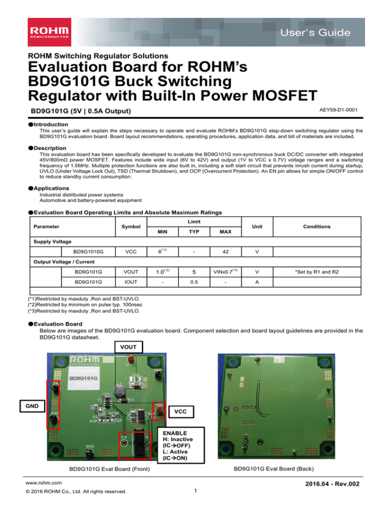
●Evaluation Board
Below are images of the BD9G101G evaluation board. Component selection and board layout guidelines are provided in the
BD9G101G datasheet.
VOUT
GND
VCC
ENABLE
H: Inactive
(IC àOFF)
L: Active
(IC àON)
BD9G101G Eval Board (Back)
BD9G101G Eval Board (Front)
www.rohm.com
© 2016 ROHM Co., Ltd. All rights reserved.
2016.04 - Rev.002
1
User’s Guide
●Board Schematic
●Board I/O
Below is a reference application circuit showing the inputs VCC and EN and the output (VOUT @5V/0.5A)
L1: 10uH
680
3.9k
●Operating Procedures
1.
2.
3.
Connect GND to a GND pin on the evaluation board
Connect VCC to the VCC pin.
i. Note: The EN pin is pulled HIGH as a default. EN needs to be set to LOW for IC operation.
The output voltage can be measured from the VOUT pin on the evaluation board. Output current can be measured with
a proper load at VOUT.
Note: The IC could be damaged if hot plugged. Therefore, make sure to power down the system before
removing or connecting the BD9G101G evaluation board.
www.rohm.com
© 2016 ROHM Co., Ltd. All rights reserved.
2016.04 - Rev.002
2
User’s Guide
●Reference Application Data
The below graphs show the efficiency, frequency response, and load characteristics of the BD9G101G eval board.
EN 10V/div
EN 10V/div
Lx
10V/div
Lx
10V/div
VOUT
1V/div
VOUT
1V/div
IOUT 0.2A/div
IOUT 0.2A/div
Start-up Characteristics
VIN=8V, IOUT=0mA ,VOUT=5V
Start-up Characteristics
VIN=8V, IOUT=500mA, VOUT=5V
EN 20V/div
Lx
10V/div
EN 20V/div
Lx
10V/div
VOUT
1V/div
VOUT
1V/div
IOUT 0.2A/div
IOUT 0.2A/div
Start-up Characteristics
VIN=12V, IOUT=0mA, VOUT=5V
Start-up Characteristics
VIN=12V, IOUT=500mA ,VOUT=5V
EN 10V/div
EN 10V/div
Lx
10V/div
Lx
10V/div
VOUT
1V/div
VOUT
1V/div
IOUT 0.2A/div
IOUT 0.2A/div
Start-up Characteristics
VIN=42V, IOUT=0mA, VOUT=5V
Start-up Characteristics
VIN=42V, IOUT=500mA, VOUT=5V
www.rohm.com
© 2016 ROHM Co., Ltd. All rights reserved.
2016.04 - Rev.002
3
User’s Guide
Io
[100mA/div]
Vout(AC)
[100mV/div]
Vout:offset 5V
10mV/div
Overshoot Voltage:46mV
UnderOvershoot Voltage:43mV
Load Response
Io=50mA⇔200mA
Lx Switching/ Vout Ripple
Io = 20mA
Vout:offset 5V
10mV/div
Phase
Gain
Lx Switching/ Vout Ripple
Io=200mA
Frequency Response
Io=100mA, VOUT=5V
100
90
Vin=12V
80
Vin=8V
70
Phase
Efficiency η [%]
60
Gain
Vin=24V
50
Vin=42V
40
30
20
10
0
1
Output Current [mA]
100
Electric Power Conversion Rate
Io=500mA, VOUT=5V
Frequency Response
Io=500mA, VOUT=5V
www.rohm.com
© 2016 ROHM Co., Ltd. All rights reserved.
10
2016.04 - Rev.002
4
1000
User’s Guide
●Application Components Selection Method
(1)
Inductors
A shield type with low DCR (DC resistance component) that satisfies the
current rating (current value Ipeak below) is recommended.
The inductance value has a significant effect on the inductor ripple current,
which becomes the source of output ripple.
As shown in the formula below, this ripple current can be made smaller
by increasing the L value of the coil and/or the switching frequency.
Ipeak =Iout + ⊿IL/2 [A]
⊿IL=
Vin-Vout
L
(1)
Vout
×
Vin
×
1
f
[A]
ΔIL
Fig 17: Inductor Current
(2)
(⊿IL: Output Ripple Current, f: Switching Frequency)
Please carry out inductor ripple design with a target of 20 to 50% of the maximum input current.
For the BD9G101G, the below inductors are recommended within the 4.7μH to 15μH range.
Recommended Inductor
TOKO DE4518C Series
TAIYO YUDEN NR4018 Series
(2)
Input Capacitor
To reduce input ripple voltage, please connect a low ESR ceramic capacitor near the VCC pin. For the BD9G101G, we
recommend a capacitance less than 4.7μF. And in the event an electrolytic capacitor is used, mount a 1μF ceramic
capacitor in parallel to prevent oscillation.
(3)
Output Capacitor
To reduce output ripple, a low ESR ceramic capacitor is recommended. And in addition to taking into account DC bias
characteristics, please provide sufficient margin with respect to the absolute maximum rated output voltage.
1
Vpp=⊿IL×
2π×f×Co
+
⊿IL×RESR
[V]
(3)
Please design in a way that it is held within Capacity Ripple Voltage.
In the BD9G101G, it is recommended a ceramic capacitor over 10μF.
(4) Output voltage setting
The internal reference voltage of the ERROR AMP is 0.75V. The output voltage is determined from the following
formula.
Vout
Csp
R1
Vo=
FB
R2
0.75V
(R1+R2)
+
+
R2
×0.75[V] ・・・ (4)
Fig 18: Output voltage setting
However, in order to prevent BSTUVLO operation during reduced power and light loads, please ensure that the sum
R1+R2 for the output resistance satisfies the following formula.
R1 + R 2 ≤ Vout × 103 ・・・ (8) (5)
・・・
Example output resistance settings: 5V output voltage → R1=3.9kΩ, R2=0.68kΩ
12V output voltage → R1=7.5kΩ, R2=0.51kΩ
www.rohm.com
© 2016 ROHM Co., Ltd. All rights reserved.
2016.04 - Rev.002
5
User’s Guide
(5)Feed-forward capacitor Csp
Please mount feed-forward capacitor in parallel to output resistance R1.
In order that a feed-forward capacitor may adjust the loop characteristic by adding the pair of a pole and zero to the
loop characteristic. A phase margin is improved and transient response speed improves.
The feed-forward capacitor Csp should use the value near the following formulas.
4.7k
× 0.15 [uF ] ・・・ (9) (6)
・・・
R1
Example Csp settings: 5V output voltage → R1=3.9kΩ, R2=0.68kΩ, Csp=0.1μF or 0.22μF
12V output voltage → R1=7.5kΩ, R2=0.51kΩ, Csp=0.1μF
Csp =
To prevent BSTUVLO operation during reduced power and light loads, we recommend connecting a feed-forward
capacitor Csp in parallel with the output resister R1. The feed-forward capacitor improves phase margin and transient
response by adding a zero-pole pair to the loop characteristics. This works to limit output fluctuation. For the
feed-forward capacitor Csp, use an output resistance value near to the following formula.
Through the above measures, BSTUVLO will not activate under light loads and VIN-VOUT<3V.
(6) Bootstrap Capacitor
To prevent malfunction of the boot pin’s internal circuit, connect a CBS=15000pF ceramic capacitor between the BST
and Lx pins.
(7) Diode
Select a Schottky barrier diode that meets withstand voltage and rated current requirements.
•
Note: The feed-forward capacitor Csp is not populated on the BD9G101G evaluation board. However, it is
recommended for designs requiring improved phase margin and transient response.
●Evaluation Board Layout Guidelines
Below are guidelines that have been tested and recommended for BD9G101G designs.
Feedback Line
Layout is a critical element of good power supply design. There are several signals paths that conduct fast changing
currents or voltages that can interact with stray inductance or parasitic capacitance to generate noise or degrade the
power supplies performance. To help eliminate these problems, the VCC pin should be bypassed to ground with a low
ESR ceramic bypass capacitor with B dielectric. Care should be taken to minimize the loop area formed by the bypass
capacitor connections, the VCC pin, and the anode of the catch diode. See Figure.45 for a PCB layout example.
In the BD9G101G, since the Lx connection is the switching node, the catch diode and output inductor should be located
close to the Lx pin and the area of the PCB conductor minimized to prevent excessive capacitive coupling. Also, the GND
area should not be connected directly to power GND or high current switch paths. The additional external components
can be placed approximately as shown.
www.rohm.com
© 2016 ROHM Co., Ltd. All rights reserved.
2016.04 - Rev.002
6
User’s Guide
●Evaluation Board BOM
Below is a table showing the bill of materials. Part numbers and supplier references are also provided.
Item
Qty
Ref
Description
Manufacturer
Part Number
Digikey P/N
1
1
CIN1
CAP CER 4.7UF 50V Y5V
1206
Murata
GRM31CF51H475ZA01L
490-1828-1-ND
2
1
CIN2
TVS DIODE 40VWM 64.5VC
SMA
Littlefuse
SMAJ40A
SMAJ40ALFTR-ND
3
1
CO2
CAP CER 10UF 10V 10% X5R
1206
Murata
GRM31CR61A106KA01L
490-1820-2-ND
4
1
CBST
Murata
GRM188R71H153KA01D
490-1514-1-ND
5
1
D1
ROHM
RB060M-60TR
RB060M-60CT-ND
6
1
SW1
E-Switch
EG1218
EG1903-ND
7
1
R1
ROHM
MCR10ERTF3901
RHM3.90KCHTR-ND
8
1
R2
RES 680 OHM 1/8W 1% 0805
SMD
ROHM
MCR10ERTF6800
RHM680CHTR-ND
9
1
Lx
INDUCT 10uH SOD-106
TOKO
DEM4518C 1235AS-H-100M
-
10
1
U1
5V, 0.5A Step-down SW Reg
w/ FET
ROHM
BD9G101G
-
CAP CER 0.015UF 50V 10%
X7R 0603
DIODE SCHOTTKY 60V 2A
PMDU
SWITCH SLIDE SPDT 30V.2A
PC MNT
RES 3.9K OHM 1/8W 1% 0805
SMD
●Revision History
Date
Revision
1.May.2013
BD9G101G
17.Mar.2016
BD9G101G-V2
Changes
NewRelease
BOM(R1,R2&CIN2)ischanged.
Noteisaddedtooperationprocedures.
www.rohm.com
© 2016 ROHM Co., Ltd. All rights reserved.
2016.04 - Rev.002
7
User’s Guide
Notes
No copying or reproduction of this document, in part or in whole, is permitted without the consent of
ROHM Co.,Ltd.
The content specified herein is subject to change for improvement without notice.
The content specified herein is for the purpose of introducing ROHM's products (herein after
"Products"). If you wish to use any such Product, please be sure to refer to the specifications which
can be obtained from ROHM upon request.
Examples of application circuits, circuit constants and any other information contained herein
illustrate the standard usage and operations of the Products. The peripheral conditions must be
taken into account when designing circuits for mass production.
Great care was taken in ensuring the accuracy of the information specified in this document.
However, should you incur any damage arising from any inaccuracy or misprint of such
information, ROHM shall bear no responsibility for such damage.
The technical information specified herein is intended only to show the typical functions of and
examples of application circuits for the Products. ROHM does not grant you, explicitly or implicitly,
any license to use or exercise intellectual property or other rights held by ROHM and other parties.
ROHM shall bear no responsibility whatsoever for any dispute arising from the use of such
technical information.
The Products specified in this document are intended to be used with general-use electronic
equipment or devices (such as audio visual equipment, office-automation equipment,
communication devices, electronic appliances and amusement devices).
The Products specified in this document are not designed to be radiation tolerant.
While ROHM always makes efforts to enhance the quality and reliability of its Products, a Product
may fail or malfunction for a variety of reasons.
Please be sure to implement in your equipment using the Products safety measures to guard
against the possibility of physical injury, fire or any other damage caused in the event of the failure
of any Product, such as derating, redundancy, fire control and fail-safe designs. ROHM shall bear
no responsibility whatsoever for your use of any Product outside of the prescribed scope or not in
accordance with the instruction manual.
The Products are not designed or manufactured to be used with any equipment, device or system
which requires an extremely high level of reliability the failure or malfunction of which may result in
a direct threat to human life or create a risk of human injury (such as a medical instrument,
transportation equipment, aerospace machinery, nuclear-reactor controller, fuel-controller or other
safety device). ROHM shall bear no responsibility in any way for use of any of the Products for the
above special purposes. If a Product is intended to be used for any such special purpose, please
contact a ROHM sales representative before purchasing.
Thank you for your accessing to ROHM product information.
More detail product information and catalogs are available, please contact us.
ROHM Customer Support System
http://www.rohm.com/contact/
www.rohm.com
© 2016 ROHM Co., Ltd. All rights reserved.
2016.04 - Rev.002
8


