Ga O (gd O )/ingaas Enhancement-mode N-channel Mosfet`s
advertisement

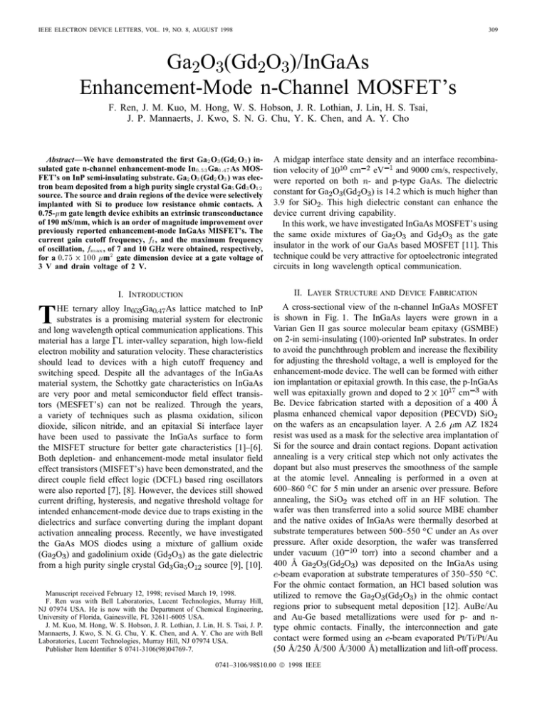
IEEE ELECTRON DEVICE LETTERS, VOL. 19, NO. 8, AUGUST 1998 309 Ga O (Gd O )/InGaAs Enhancement-Mode n-Channel MOSFET’s F. Ren, J. M. Kuo, M. Hong, W. S. Hobson, J. R. Lothian, J. Lin, H. S. Tsai, J. P. Mannaerts, J. Kwo, S. N. G. Chu, Y. K. Chen, and A. Y. Cho Abstract—We have demonstrated the first Ga2 O3 (Gd2 O3 ) insulated gate n-channel enhancement-mode In0:53 Ga0:47 As MOSFET’s on InP semi-insulating substrate. Ga2 O3 (Gd2 O3 ) was electron beam deposited from a high purity single crystal Ga5 Gd3 O12 source. The source and drain regions of the device were selectively implanted with Si to produce low resistance ohmic contacts. A 0.75-m gate length device exhibits an extrinsic transconductance of 190 mS/mm, which is an order of magnitude improvement over previously reported enhancement-mode InGaAs MISFET’s. The current gain cutoff frequency, ft , and the maximum frequency of oscillation, fmax , of 7 and 10 GHz were obtained, respectively, for a 0:75 2 100 m2 gate dimension device at a gate voltage of 3 V and drain voltage of 2 V. A midgap interface state density and an interface recombinacm eV and 9000 cm/s, respectively, tion velocity of were reported on both - and p-type GaAs. The dielectric constant for Ga O (Gd O ) is 14.2 which is much higher than 3.9 for SiO . This high dielectric constant can enhance the device current driving capability. In this work, we have investigated InGaAs MOSFET’s using the same oxide mixtures of Ga O and Gd O as the gate insulator in the work of our GaAs based MOSFET [11]. This technique could be very attractive for optoelectronic integrated circuits in long wavelength optical communication. I. INTRODUCTION II. LAYER STRUCTURE AND DEVICE FABRICATION HE ternary alloy In Ga As lattice matched to InP substrates is a promising material system for electronic and long wavelength optical communication applications. This material has a large L inter-valley separation, high low-field electron mobility and saturation velocity. These characteristics should lead to devices with a high cutoff frequency and switching speed. Despite all the advantages of the InGaAs material system, the Schottky gate characteristics on InGaAs are very poor and metal semiconductor field effect transistors (MESFET’s) can not be realized. Through the years, a variety of techniques such as plasma oxidation, silicon dioxide, silicon nitride, and an epitaxial Si interface layer have been used to passivate the InGaAs surface to form the MISFET structure for better gate characteristics [1]–[6]. Both depletion- and enhancement-mode metal insulator field effect transistors (MISFET’s) have been demonstrated, and the direct couple field effect logic (DCFL) based ring oscillators were also reported [7], [8]. However, the devices still showed current drifting, hysteresis, and negative threshold voltage for intended enhancement-mode device due to traps existing in the dielectrics and surface converting during the implant dopant activation annealing process. Recently, we have investigated the GaAs MOS diodes using a mixture of gallium oxide (Ga O ) and gadolinium oxide (Gd O ) as the gate dielectric from a high purity single crystal Gd Ga O source [9], [10]. A cross-sectional view of the n-channel InGaAs MOSFET is shown in Fig. 1. The InGaAs layers were grown in a Varian Gen II gas source molecular beam epitaxy (GSMBE) on 2-in semi-insulating (100)-oriented InP substrates. In order to avoid the punchthrough problem and increase the flexibility for adjusting the threshold voltage, a well is employed for the enhancement-mode device. The well can be formed with either ion implantation or epitaxial growth. In this case, the p-InGaAs cm with well was epitaxially grown and doped to Be. Device fabrication started with a deposition of a 400 Å plasma enhanced chemical vapor deposition (PECVD) SiO on the wafers as an encapsulation layer. A 2.6 m AZ 1824 resist was used as a mask for the selective area implantation of Si for the source and drain contact regions. Dopant activation annealing is a very critical step which not only activates the dopant but also must preserves the smoothness of the sample at the atomic level. Annealing is performed in a oven at 600–860 C for 5 min under an arsenic over pressure. Before annealing, the SiO was etched off in an HF solution. The wafer was then transferred into a solid source MBE chamber and the native oxides of InGaAs were thermally desorbed at substrate temperatures between 500–550 C under an As over pressure. After oxide desorption, the wafer was transferred torr) into a second chamber and a under vacuum ( 400 Å Ga O (Gd O ) was deposited on the InGaAs using -beam evaporation at substrate temperatures of 350–550 C. For the ohmic contact formation, an HCl based solution was utilized to remove the Ga O (Gd O ) in the ohmic contact regions prior to subsequent metal deposition [12]. AuBe/Au and Au-Ge based metallizations were used for p- and ntype ohmic contacts. Finally, the interconnection and gate contact were formed using an -beam evaporated Pt/Ti/Pt/Au (50 Å/250 Å/500 Å/3000 Å) metallization and lift-off process. T Manuscript received February 12, 1998; revised March 19, 1998. F. Ren was with Bell Laboratories, Lucent Technologies, Murray Hill, NJ 07974 USA. He is now with the Department of Chemical Engineering, University of Florida, Gainesville, FL 32611-6005 USA. J. M. Kuo, M. Hong, W. S. Hobson, J. R. Lothian, J. Lin, H. S. Tsai, J. P. Mannaerts, J. Kwo, S. N. G. Chu, Y. K. Chen, and A. Y. Cho are with Bell Laboratories, Lucent Technologies, Murray Hill, NJ 07974 USA. Publisher Item Identifier S 0741-3106(98)04769-7. 0741–3106/98$10.00 1998 IEEE 310 IEEE ELECTRON DEVICE LETTERS, VOL. 19, NO. 8, AUGUST 1998 Fig. 1. A cross-sectional view of a p-channel InGaAs MOSFET. Fig. 3. Comparison of the extrinsic transconductance for this work with previous reported data. Fig. 2. The drain I InGaAs MOSFET. 0V characteristics of a typical 1 2 50 m2 n-channel III. DEVICE RESULTS Fig. 2 illustrates the drain curves of a typical m gate geometry enhancement-mode n-channel InGaAs MOSFET passivated with Ga O (Gd O ). The gate to V in steps of 0.5 V and voltage is varied from , is 0.5 V. The p-well is externally the threshold voltage, connected to source contact through the p-well contact. The breakdown is around 2.5 V which is limited by the low doping level in the p-well. The device shows no leakage current and no hysteresis. The device was stressed at 1.5 V of drain voltage and 3 V of gate voltage for over 4 h. The drain current only decreased less than 1% and intended to reach the saturation after first 10 min stress. An effective mobility of 470 cm /Vs which is limited by the parasitic resistance and can be improved by optimizing the implant condition is derived from the variation of drain , versus gate voltage at a small drain voltage conductance, ( 0 V). Fig. 3 illustrates the comparison among the current technology and previous works on extrinsic transconductance, Fig. 4. The rf frequency response as a function of the gate voltage of a 0:75 100 m2 gate dimension InGaAs n-MOSFET. 2 , for different gate length. Generally, the is higher for depletion-mode devices because the current density is determined by the doping in the channel layer. For enhancementmode devices, the drain current is induced by bending the conduction band and creating the inversion channel, therefore, is dominated by the quality of the surface the extrinsic state density, the parasitic resistance, and the smoothness of the oxide-semiconductor interface. A maximum extrinsic of transconductance of 190 mS/mm is obtained at a of 3 V, respectively, for a device with gate 2 V and m . Our work clearly exhibits dimension of improved performance over previously reported data. The current gain cutoff frequency, , and the maximum , of 7 and 10 GHz were obtained, frequency of oscillation, m gate dimension device at a respectively, for a gate voltage of 3 V and drain voltage of 2 V. The frequency responses can be further improved by reducing the device capacitance by using mesa isolation to lower the extrinsic capacitance and a self-aligned gate process to reduce the source/drain-to-gate capacitance. Fig. 4 shows the frequency REN et al.: Ga O (Gd O )/InGaAs ENHANCEMENT-MODE N-CHANNEL MOSFET’S response of the same device as a function of the gate voltage. and remain fairly constant once the maximum Both value is reached, unlike the conventional GaAs MESFET or HEMT’s, which will roll-off when the Schottky gate starts 0.7 V). This is a typical characteristic of the to turn on ( MOSFET since the device capacitance, which is determined by the device dimension, oxide thickness, and the dielectric constant of the oxide, remains constant in the strong inversion region. This characteristic can be very useful in analog designs. In conclusion, we have demonstrated the first Ga O (Gd O ) insulated gate n-channel enhancementmode In Ga As MOSFET’s on an InP semi-insulating substrate. The 0.75 m gate length device exhibits an extrinsic transconductance of 190 mS/mm which is an order of magnitude improvement over previously reported values. Further work to reduce gate and drain capacitance is expected to result in improved rf performance. ACKNOWLEDGMENT The authors thank G. Georgiou for the illuminating discussion and T. R. Fullowan for technical support. REFERENCES [1] A. S. H. Liao, B. Tell, R. F. Leheny, and T. Y. Chang, “In0:53 Ga0:47 As n-channel native oxide inversion mode field-effect transistor,” Appl. Phys. Lett., vol. 41, pp. 280–281, 1982. [2] H. H. Wieder, A. R. Clawson, D. I. Elder, and D. A. Collins, “Inversionmode insulated gate Ga0:47 In0:53 As field-effect transistors,” IEEE Electron Device Lett., vol. EDL-2, pp. 73–75, 1981. 311 [3] C. Watanabe, S. Kinoshita, K. Furuya, and Y. Miyamoto, “GaInAs/InP MOSFET by organometallic vapor phase epitaxy and water oxidation techniques,” Trans. IECE Jpn., 1986, vol. E69, pp. 779–781. [4] J. Splettstößer, F. Schulte, A. Trasser, D. Schmitz, and H. Beneking, “High speed MISFET’s grown by metal organic vapor phase epitaxy,” in 19th Europ. Solid State Dev. Res. Conf., Berlin, Germany, 1989, pp. 267–270. [5] D. S. L. Mui, Z. Wang, D. Biswas, A. L. Demirel, N. Teraguchi, J. Reed, and H. Morko, “Si3 N4 /Si/In0:53 Ga0:47 As depletion-mode metalinsulator-semiconductor field-effect transistors with improved stability,” Appl. Phys. Lett., vol. 62, pp. 3291–3293, 1993. [6] P. D. Gardner, S. Y. Narayan, and Y. H. Yun, “Characterization of the low-temperature deposited SiO2 -GaInAs metal/insulator/semiconductor interface,” Thin Solid Films, vol. 117, pp. 173–190, 1984. [7] F. Schulte, C. Werres, J. Splettstößer, D. Schmitz, R. Tuzinski, K. Heime, and H. Beneking, “Analog and digital performance of MISFET’s on p- and n-GaInAs,” 4th Intern. Conf. InP Rel. Mat., 1992, pp. 503–506. [8] L. C. Upadhyayula, P. D. Gardner, S. G. Liu, and S. Y. Narayan, “Inversion-mode GaInAs MISFET ring oscillators,” IEEE Electron Device Lett., vol. EDL-7, pp. 390–392, 1986. [9] M. Hong, M. Passlack, J. P. Mannaerts, J. Kwo, S. N. G. Chu, N. Moriya, S. Y. Hou, and V. J. Fratello, “Low interface state density oxide-GaAs structures fabricated by in-situ molecular beam epitaxy,” J. Vac. Sci Technol., vol. B14, pp. 2297–2300, 1996. [10] M. Passlack, M. Hong, J. P. Mannaerts, R. L. Opila, S. N. G. Chu, N. Moriya, F. Ren, and J. R. Kwo, “Low dit , thermodynamically stable Ga2 O3 -GaAs interfaces: Fabrication, characterization, and modeling,” IEEE Trans. Electron Deices., vol. 44, pp. 214–225, 1997. [11] F. Ren, M. Hong, W. S. Hobson, J. M. Kuo, J. R. Lothian, J. P. Mannaerts, J. Kwo, S. N. G. Chu, Y. K. Chen, and A. Y. Cho, “Demonstration of enhancement-mode p- and n-channel GaAs MOSFET’s with as gate oxide,” Solid State Electron., vol. 41, p. 1751, 1997. [12] F. Ren, M. Hong, J. P. Mannaerts, J. R. Lothian, and A. Y. Cho, “Wet chemical and plasma etching of Ga2 O3 (Gd2 O3 ),” J. Electrochem. Soc., vol. 144, pp. L239–241, 1997.


