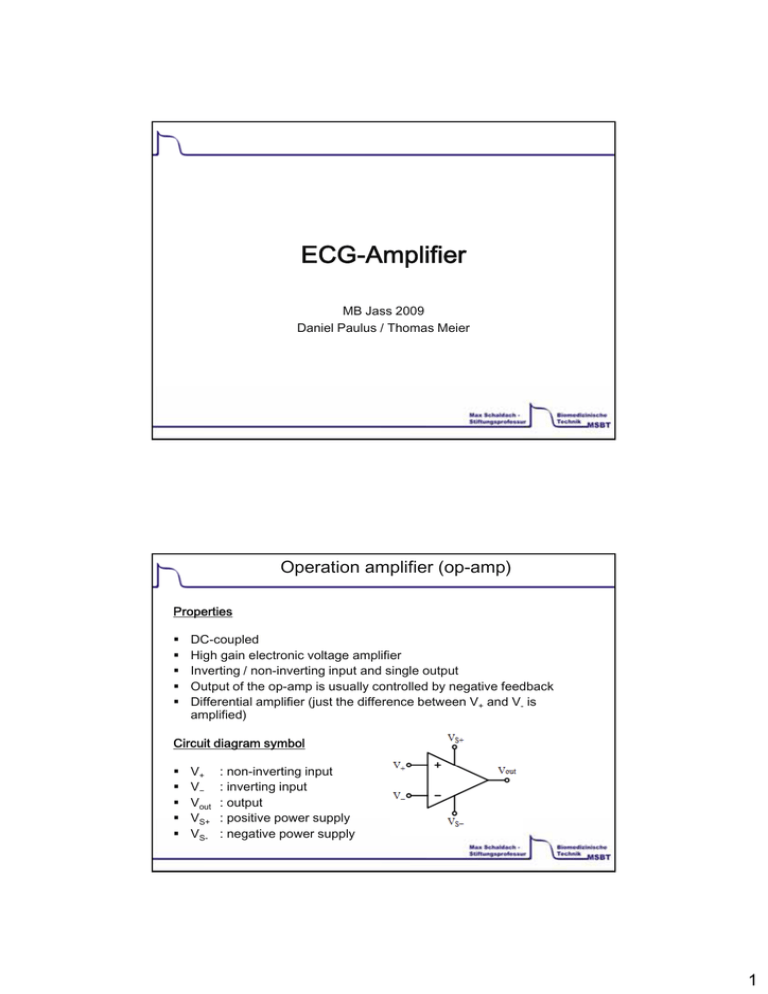
ECG-Amplifier
advertisement

ECG-Amplifier MB Jass 2009 Daniel Paulus / Thomas Meier Operation amplifier (op-amp) Properties DC-coupled g ga gain e electronic ec o c voltage o age a amplifier p e High Inverting / non-inverting input and single output Output of the op-amp is usually controlled by negative feedback Differential amplifier (just the difference between V+ and V- is amplified) Circuit diagram symbol V+ V− Vout VS+ VS- : non-inverting input : inverting input : output : positive power supply : negative power supply 1 Ideal op-amp Properties for an ideal op-amp Zero output impedance (Rout = 0) I fi i open-loop Infinite l gain i Infinite input impedance (Rin= ∞) Zero offset voltage Zero noise Common mode gain Ideal op-amps amplify only the voltage difference in its inputs Real op-amps amplify also voltage that is common to both inputs (common mode gain) Minimizing this common mode gain (i.e. maximizing the common mode rejection ratio, ’CMRR’) is important for most applications 2 Non-inverting Amplifier Very high input impedance Small output impedance Gain: Ua (1 R2 )Ue R1 Amplifies Ue regarding to the ground and not the difference between two different voltages Instrumentation amplifier Type of differential amplifier (usually 3 op-amps) Input buffers Output controlled by negative feedback Characteristics Very low DC offset Low drift Low signal noise Veryy high g open-loop p pg gain Very high common-mode rejection ratio Very high input impedance 3 Description of the INA 118 INA118: Low power, general purpose instrumentation amplifier offering excellent accuracy 3 op-amps (small size) Current-feedback input provides high gain even at high frequencies INA118 Electrical Features Low offset voltage (50 µV) L Low temperature d drift if (0 (0.5 µV/K) V/K) High common-mode-rejection (110dB) at high gain Low quiescent current (350 µA at ± 1.35V supply) Single external resistor sets any gain from 1 to 10,000 Internal input protection can withstand up to ±40V without damage 4 Instrumentation amplifier INA118 Circuit of the Instrumentation amplifier used in our ECG-circuit Gain: G 1 50k RG Performance curves (INA118) Gain of the amplifier plotted against the frequency C Common-mode d rejection j ti as a function of the frequency 5 Electrocardiogram Properties of the electric signals on the skin: AC C ssignal g a with ba bandwidth d d of o 0 0.05 05 to o 100 00 Hz,, so sometimes e es up to o 1 kHz About 1 mV peak-to-peak amplitude External noise at higher frequencies 50/60 Hz interference Common-mode voltages (common to all electrodes) Circuit schematic of an ECG PC 6 ECG The common-mode voltage is comprised of two parts: 1) 2) 50- or 60-Hz interferences DC electrode l t d offset ff t potential t ti l Other noise or higher frequencies within the biophysical bandwidth come from: Movement artifacts that change the skin-electrode interface Muscle contraction or electromyographic spikes Respiration Electromagnetic interferences Noise from other electronic devices that couple into the input ECG Some noise can be cancelled with a high-input-impedance instrumentation amplifier (INA) → removes the AC line noise common to both inputs → amplifies the remaining unequal signals present on the inputs Let’s detect an ECG with our construction 7 Filter Device for manipulating the frequency content of a given signal Fourier Inverse Fourier Passive analog filter: RC network Uin Uoutideal 1 kΩ 8 μF real real ideal Impedance of capacitor: Z = 1/(ωC) -> fco = (RC)-1 8 Active analog filter real Complex circuit Once it’s set up, it’s hard to change ideal Fourier Transform Direct manipulation of frequency content in the frequency domain is suitable for post processing only! (Whole signal has to be stored in memory) Possible solution for in-stream processing: windowing Problems: •High computational cost •Frequency spectrum limited by window size Manipulation in Fourier space 9 Convolution Possibility: Operating in time domain Bring transfer function to time domain by inverse Fourier Transform (Impulse response) Cut function to realise convolution of impulse response & signal as sum Y (t ) T ( ) X (t )d Implementation: FIR Simple implementation: convolution implemented as sum h is the filter kernel of length q q Y ( z ) h ( m) X ( z m) m 0 Major drawback: very long filters necessary to achieve good performance 10 Implementation: IIR Recursive implementation: both input and response are considered Y ( z) q 1 p d i X ( z i ) g jY ( z j ) a0 i 0 j 0 Advantage: Less coefficients required in comparison to FIR filters to get same perfomance Digital Filter: Transfer function real ideal 11 Advantages/Disadvantages Advantages Disadvantages Digital filters can realise FIR filters need to be large to frequency responses be effective (many operations) practically not achievable with IIR filters may be unstable analog filters because of feed back loop No tolerance of circuit The ADC stage creates components deterministic quantisation error No complex circuitry (just a which is due to digital storage number of coefficients needed) and computation limitations sample l rate t limitation li it ti ((analog l filters do not have to sample!) Filter design is not a simple task 12


