IXA20PT1200LB
tentative
XPT IGBT
VCES
= 2x 1200 V
I C25
=
28 A
VCE(sat) =
1.8 V
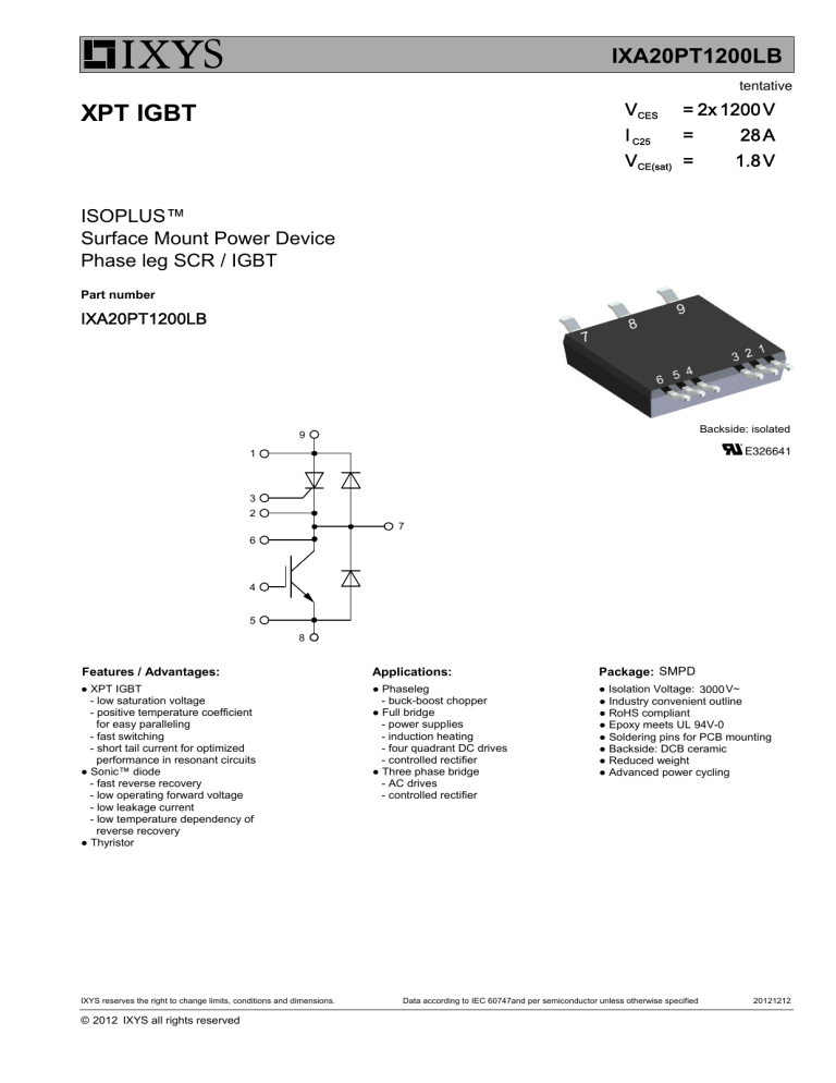
ISOPLUS™
Surface Mount Power Device
Phase leg SCR / IGBT
Part number
IXA20PT1200LB
Backside: isolated
9
E326641
1
3
2
7
6
4
5
8
Features / Advantages:
Applications:
Package: SMPD
● XPT IGBT
- low saturation voltage
- positive temperature coefficient
for easy paralleling
- fast switching
- short tail current for optimized
performance in resonant circuits
● Sonic™ diode
- fast reverse recovery
- low operating forward voltage
- low leakage current
- low temperature dependency of
reverse recovery
● Thyristor
● Phaseleg
- buck-boost chopper
● Full bridge
- power supplies
- induction heating
- four quadrant DC drives
- controlled rectifier
● Three phase bridge
- AC drives
- controlled rectifier
● Isolation Voltage: 3000 V~
● Industry convenient outline
● RoHS compliant
● Epoxy meets UL 94V-0
● Soldering pins for PCB mounting
● Backside: DCB ceramic
● Reduced weight
● Advanced power cycling
IXYS reserves the right to change limits, conditions and dimensions.
© 2012 IXYS all rights reserved
Data according to IEC 60747and per semiconductor unless otherwise specified
20121212
IXA20PT1200LB
tentative
Ratings
IGBT
Symbol
VCES
Definition
collector emitter voltage
VGES
max. DC gate voltage
VGEM
max. transient gate emitter voltage
I C25
collector current
Conditions
min.
TVJ =
typ.
25°C
TC = 25°C
I C80
2.1
V
6.5
V
0.1
mA
gate emitter threshold voltage
I C = 0.6 mA; VGE = VCE
TVJ = 25°C
I CES
collector emitter leakage current
VCE = VCES; VGE = 0 V
TVJ = 25°C
TVJ = 25°C
1.8
TVJ = 125 °C
turn-on delay time
tr
current rise time
t d(off)
turn-off delay time
tf
current fall time
Eon
turn-on energy per pulse
Eoff
turn-off energy per pulse
RBSOA
reverse bias safe operating area
I CM
inductive load
5.4
5.9
TVJ = 125 °C
VGE = ±15 V; R G = 56 Ω
short circuit safe operating area
VCEmax = 1200 V
t SC
short circuit duration
VCE = 900 V; VGE = ±15 V
R G = 56 Ω; non-repetitive
I SC
short circuit current
R thJC
thermal resistance junction to case
R thCH
thermal resistance case to heatsink
nA
48
nC
70
ns
40
ns
250
ns
100
ns
1.55
mJ
1.7
mJ
TVJ = 125 °C
VCEmax = 1200 V
SCSOA
mA
0.1
500
VCE = 600 V; IC = 15 A
VGE = ±15 V; R G = 56 Ω
V
2
TVJ = 125 °C
t d(on)
A
A
VGE(th)
VCE = 600 V; VGE = 15 V; IC = 15 A
V
28
W
I C = 15 A; VGE = 15 V
VGE = ±20 V
tbd
20
collector emitter saturation voltage
total gate charge
V
100
VCE(sat)
gate emitter leakage current
±20
TC = 25°C
total power dissipation
Q G(on)
Unit
V
TC = 80 °C
Ptot
I GES
max.
1200
TVJ = 125 °C
45
A
10
µs
A
60
1.25 K/W
K/W
0.40
Diode
VRRM
max. repetitive reverse voltage
TVJ = 25°C
1200
V
I F25
forward current
TC = 25°C
32
A
TC = 80 °C
22
A
TVJ = 25°C
2.24
V
0.03
mA
I F 80
VF
forward voltage
I F = 20 A
IR
reverse current
VR = VRRM
TVJ = 125°C
TVJ = 25°C
TVJ = 125°C
Q rr
reverse recovery charge
I RM
max. reverse recovery current
t rr
reverse recovery time
E rec
reverse recovery energy
R thJC
thermal resistance junction to case
R thCH
thermal resistance case to heatsink
IXYS reserves the right to change limits, conditions and dimensions.
© 2012 IXYS all rights reserved
VR = 600 V
-di F /dt = 400 A/µs
IF = 20 A; VGE = 0 V
TVJ = 125°C
V
1.90
0.12
mA
3
µC
20
A
350
ns
0.7
mJ
1.5 K/W
0.5
Data according to IEC 60747and per semiconductor unless otherwise specified
K/W
20121212
IXA20PT1200LB
tentative
Ratings
Thyristor
Conditions
Symbol
V RSM/DSM
Definition
V RRM/DRM
max. repetitive reverse/forward blocking voltage
I R/D
reverse current, drain current
VR/D = 1200 V
VR/D = 1200 V
VT
forward voltage drop
IT =
15 A
IT =
30 A
IT =
15 A
IT =
30 A
min.
max. non-repetitive reverse/forward blocking voltage
I TAV
average forward current
TC = 80°C
I T(RMS)
RMS forward current
180 sine
VT0
threshold voltage
rT
slope resistance
R thJC
thermal resistance junction to case
thermal resistance case to heatsink
Ptot
total power dissipation
I TSM
max. forward surge current
max.
1300
TVJ = 25°C
1200
V
TVJ = 25°C
50
µA
TVJ = 125°C
5
mA
TVJ = 25°C
1.42
V
1.77
V
TVJ = 125 °C
1.37
V
1.86
V
18
A
28
A
T VJ = 150 °C
TVJ = 150 °C
for power loss calculation only
R thCH
typ.
Unit
V
TVJ = 25°C
0.87
V
32.9
mΩ
1.7
0.57
K/W
K/W
TC = 25°C
74
W
t = 10 ms; (50 Hz), sine
TVJ = 45°C
200
A
t = 8,3 ms; (60 Hz), sine
VR = 0 V
215
A
t = 10 ms; (50 Hz), sine
TVJ = 150 °C
170
A
t = 8,3 ms; (60 Hz), sine
VR = 0 V
185
A
t = 10 ms; (50 Hz), sine
TVJ = 45°C
200
A²s
t = 8,3 ms; (60 Hz), sine
t = 10 ms; (50 Hz), sine
VR = 0 V
190
A²s
TVJ = 150 °C
145
A²s
t = 8,3 ms; (60 Hz), sine
VR = 0 V
140
A²s
CJ
junction capacitance
VR =
TVJ = 25°C
PGM
max. gate power dissipation
t P = 30 µs
PGAV
average gate power dissipation
(di/dt) cr
critical rate of rise of current
I²t
value for fusing
0 V f = 1 MHz
0
T C = 150 °C
t P = 300 µs
TVJ = 125°C; f = 50 Hz
pF
10
W
5
W
0.5
W
repetitive, IT =
20 A
100 A/µs
non-repet., IT =
20 A
500 A/µs
t P = 200 µs; di G /dt = 0.3 A/µs;
IG =
(dv/dt) cr
critical rate of rise of voltage
0.3 A; VD = ⅔ VDRM
VD = ⅔ VDRM
TVJ = 125°C
500 V/µs
TVJ = 25 °C
1.5
V
TVJ = -40 °C
2.5
V
R GK = ∞; method 1 (linear voltage rise)
VGT
I GT
gate trigger voltage
gate trigger current
VD = 6 V
VD = 6 V
TVJ = 25 °C
25
mA
TVJ = -40 °C
50
mA
VD = ⅔ VDRM
TVJ = 125 °C
0.2
V
4
mA
TVJ = 25 °C
75
mA
TVJ = 25 °C
50
mA
TVJ = 25 °C
2
µs
VGD
gate non-trigger voltage
I GD
gate non-trigger current
IL
latching current
t p = 10 µs
IH
holding current
VD = 6 V R GK = ∞
t gd
gate controlled delay time
IG =
turn-off time
0.3 A/µs
VD = ½ VDRM
IG =
tq
0.3 A; di G /dt =
0.3 A; di G /dt =
0.3 A/µs
VR = 100 V; I T = 20 A; VD = ⅔ VDRM TVJ = 150 °C
di/dt = 10 A/µs; dv/dt =
IXYS reserves the right to change limits, conditions and dimensions.
© 2012 IXYS all rights reserved
40
µs
20 V/µs; t p = 200 µs
Data according to IEC 60747and per semiconductor unless otherwise specified
20121212
IXA20PT1200LB
tentative
Package
Ratings
SMPD
Symbol
I RMS
Definition
Conditions
RMS current
per terminal
Tstg
storage temperature
T VJ
virtual junction temperature
min.
typ.
max.
100
Unit
A
-55
150
°C
-55
150
°C
Weight
FC
8.5
40
mounting force with clip
d Spp/App
d Spb/Apb
VISOL
~
1.6
mm
4.0
mm
3000
V
2500
V
50/60 Hz, RMS; IISOL ≤ 1 mA
UL Logo
~
Part number
~
I
X
A
20
PT
1200
LB
Backside DCB
Part number
Date code
XXXXXXXXXX
yywwA
Assembly line
N
terminal to backside
t = 1 second
t = 1 minute
130
terminal to terminal
creepage distance on surface | striking distance through air
isolation voltage
g
=
=
=
=
=
=
=
IGBT
XPT IGBT
Gen 1 / std
Current Rating [A]
Phase leg SCR / IGBT
Reverse Voltage [V]
SMPD-B
Data Matrix Code
Digits
1 to 19:
20 to 23:
24 to 25:
26 to 31:
32:
33 to 36:
Part #
Date Code
Assembly line
Lot #
Split Lot
Individual #
Pin 1 identifier
Ordering
Standard
Part Number
IXA20PT1200LB
Equivalent Circuits for Simulation
I
V0
R0
Marking on Product
IXA20PT1200LB
Delivery Mode
Blister
Tape & Reel
IGBT
Diode
V 0 max
threshold voltage
0.87
1.1
1.2
V
R 0 max
slope resistance *
32.9
90
45
mΩ
© 2012 IXYS all rights reserved
Code No.
T VJ = 150°C
* on die level
Thyristor
IXYS reserves the right to change limits, conditions and dimensions.
Quantity
45
200
Data according to IEC 60747and per semiconductor unless otherwise specified
20121212
IXA20PT1200LB
tentative
Outlines SMPD
A(8:1)
2)
5,5 ` 0,1
(6x) 1 `0,05
0 + 0,15
2°
c 0,1
0,5 ` 0,1
1)
18 `0,1
seating plane
(3x) 2 ` 0,05
9 ` 0,1
2)
4 ` 0,05
8
9
23 ` 0,2
32,7 `0,5
2 `0,2
7
0,55 ` 0,1
4,85 ` 0,2
25 `0,2
3)
c 0,05
6 5 4
A
3 2 1
Pin number
2,75 ` 0,1
5,5 ` 0,1
13,5 `0,1
16,25 `0,1
19 `0,1
Notes:
1) potrusion may add 0.2 mm max. on each side
2) additional max. 0.05 mm per side by punching misalignement
or overlap of dam bar or bending compression
3) DCB area 10 to 50 µm convex;
position of DCB area in relation to plastic rim: ±25 µm
(measured 2 mm from Cu rim)
4) terminal plating: 0.2 - 1 µm Ni + 10 - 25 µm Sn (gal v.)
cutting edges may be partially free of plating
9
1
3
2
7
6
4
5
8
IXYS reserves the right to change limits, conditions and dimensions.
© 2012 IXYS all rights reserved
Data according to IEC 60747and per semiconductor unless otherwise specified
20121212
