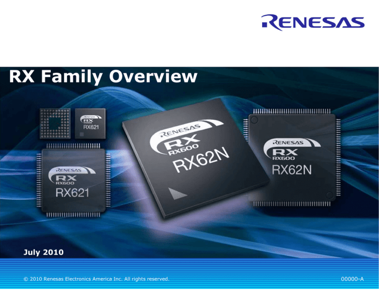
RX Family Overview
Renesas Electronics America Inc.
July 2010
© 2010 Renesas Electronics America Inc. All rights reserved.
00000-A
The New Renesas Electronics
Worldwide MCU Market Share
0%
Renesas
Electronics
10%
Renesas Electronics
Renesas
Technology
20%
30%
40%
#1 MCU Worldwide Supplier
NEC Electronics
Own design
Freescale Semiconductor
Samsung Electronics
Microchip Technology
Own fab
Own flash technology
Texas Instruments
Own CPU architectures
Infineon Technologies
STMicroelectronics
Fujitsu Microelectronics
NXP
Based on Gartner Worldwide Semiconductor Market Share Database; March 2010 results
2
© 2010 Renesas Electronics America Inc. All rights reserved.
32-bit
32-bit
32-bit
H8S/SX
78K0
R8C
50MHz
32-bit
V850ES
General
Purpose
32-bit
32-bit
Ultra Low
Power
32-bit
100MHz
SH-2A
200MHz
50MHz
V850ES
RX
TFT LCD
Control
R32C
200MHz
8-bit
32-bit
200MHz
20MHz
240MHz
SH-3
8-bit
SH-2A
32-bit
High-end
Connectivity
600MHz
SH-4
16-bit
32-bit
SH-4A
78K0R
16-bit
Application
Processor
32-bit
Renesas MCU and MPU Solutions
M16C
20MHz
32MHz
50MHz
10MHz
20MHz
Application Focused Solutions
3
WiFi
Motor Control
SH, RX, R8C
SH, RX, R8C
Capacitive
Touch
© 2010 Renesas Electronics America Inc. All rights reserved.
R8C
Industrial CAN
Lighting
R8C, R32C, SH
78K0
The RX Concept
Extreme performance
32-bit RX CPU core
165 DMIPS | 100 MHz
FPU & DSP
+
Extreme flash technology
90nm MONOS cell
Zero-Wait 100 MHz
+
Extreme code efficiency
CISC instructions
+
Extreme power efficiency
4
© 2010 Renesas Electronics America Inc. All rights reserved.
500µ
µA per MHz Fully Active
2.5µ
µA Deep Standby
Up to 165 DMIPS
Dhrystone DMIPS per MHz
32-bit RX CPU
ARM7
ARM9
Cortex-M3
Cortex-M4
• Mostly single clock instructions
• 5-stage execution pipeline
RX
• Ultra fast 5-cycle interrupts
1.0
1.65 DMIPS/MHz
1.5
Note: Dhrystone 2.1 numbers for ARM
processors taken from www.arm.com
32-bit FPU
• Single precision
• IEEE-754 compliant
• Direct access to General Registers
DSP
• Repeated Multiply & Accumulate 80-bits
• Multiply & Accumulate 48-bits
• Barrel shifter 32-bits
Multiple busses
• Enhanced Harvard bus
• Internal DTC and DMA controllers
• External bus with DMA controller
5
© 2010 Renesas Electronics America Inc. All rights reserved.
Perfect Blend of CISC and RISC
CPU Execution Time = # of Instructions x Cycles Per Instruction x Cycle Time
Traditional CISC
Reduces # of Instructions in Memory
Any instruction references memory
Many instructions
Many addressing modes
Variable instruction formats
Program code size small
Less-to-no pipelining
Single register set
Multi-clock instructions
Longer interrupt response
6
RX is Best of Both Worlds
Memory-to-memory operations
73 basic instructions + DSP + FPU
10 addressing modes
Traditional RISC
Reduces # of Clocks Per Instruction
Only load/store references memory
Few instructions
Few addressing modes
8, 16, 32, and 64-bit instructions
Fixed instruction formats
Up to 28% code size reductions
Program code size large
5-stage pipeline
16 x 32-bit registers
Highly pipelined
Multiple register sets
Single-clock instructions
Single-clock instructions
Ultra fast 5-cycle interrupt latency
Faster interrupt response
© 2010 Renesas Electronics America Inc. All rights reserved.
FPU Directly Accesses General Registers
Typical Operation
RX Operation
General Registers
General
Registers
No Load/Store
Instructions
Needed
FloatingPoint Unit
Load/Store
Dedicated
Data
Registers
Smaller code size
FloatingPoint Unit
7
© 2010 Renesas Electronics America Inc. All rights reserved.
Up to 50% higher
performance
Multiple Busses Increase Data Throughput
RX CPU
Instruction Bus
Operand Bus
Flash
RAM
Main Bus 1
Three simultaneous operations
DMA
controller
1. RX CPU executing out of Flash
2. ADC storing data to RAM
Main Bus 2
External
External DMA
DMA
controller
controller
External bus control
Peripheral Bus
3. External Memory sending data
to External LCD
TMR SCI ADC .
External Bus
External
LCD
External
Memory
RX CPU
DMA controller
External DMA controller
8
© 2010 Renesas Electronics America Inc. All rights reserved.
Zero Wait-state 100MHz Flash
90nm MONOS cell
• 1.5B Flash MCUs shipped
• 10ns access time
Processing performance
RX with 100
MHz flash
Processing performance gap
Competing MCU
with 30 MHz flash
3 or more
2 wait cycles
1 wait cycle
30 MHz
9
100 MHz
© 2010 Renesas Electronics America Inc. All rights reserved.
MCU operating frequency
Up to 28% Code Size Reduction
Code size (relative)
Motor control
28% less
Data communication
19% less
Data conversion
17% less
Real-time control
25% less
System control
25% less
Addressing mode
advantages on RX
• Ten modes available
• Support for Array operations
• Memory-to-Memory operations
Example: Moving data in memory
1.0
= RX600
Traditional RISC
= Cortex-M3 based MCU
Note: Internal benchmark test, your results may vary
RX
LDR r3, [r1] 2 bytes
STR r3, [r2] 2 bytes
MOV [r1], [r2] 2 bytes
Number of Cycles = 4
Number of Cycles = 3
Code size = 4 bytes
Code size = 2 bytes
Direct Memory-to-Memory operation allows RX to avoid
lengthy load/store operations and results in smaller code size
10
© 2010 Renesas Electronics America Inc. All rights reserved.
Up to 43% Power Reduction
Milliwatts per DMIPS
43% less
Low power modes
• 500µ
µA per MHz in Run Mode
1.0
2.0
= RX600
= Cortex-M3 based MCU
• All Peripherals ON
• 2.5µ
µA in Deep Software Standby
• RX63x, RTC ON
Note: Derived from IDD specifications
stated in product datasheets
Low power design techniques
• Clock gating
• Low power HVT transistors
• Power gating
Animation Fix
11
© 2010 Renesas Electronics America Inc. All rights reserved.
Applications
Building
Automation
Medical
eMetering
Motor Control
Home
Appliances
12
© 2010 Renesas Electronics America Inc. All rights reserved.
RX Family Roadmap
200
Max
MHz
RX600
100
50
65 nm
100MHz+
RX600 Series
32 Bit, 90nm
Extreme High Performance
High Efficiency
H8SX
32 Bit
H8S
16 Bit
R32C
RX200 Series
M16C
32 Bit, 130 nm
High Performance
Ultra-Low Power
32 Bit
Family
16 Bit
Existing MCUs
2010
2MB
2011
2012
Flash
RX600 Series - 100Mhz Extreme Performance
1MB
Migration
Within RX
Family
512KB
Common CPU &
Peripherals
384KB
256KB
128KB
64KB
32KB
RX200 Series - 50Mhz Ultra Low Power
Pins
36
13
© 2010 Renesas Electronics America Inc. All rights reserved.
48
64
80/85
100
112
144/145
176
Animation Fix
RX600 Product Roadmap
RX62T
RX63T
64KB – 256KB Flash
8KB – 16KB SRAM
64 - 112 pins
Dual Motor Control, Analog, CAN
32KB – 512KB Flash
6KB – 96KB SRAM
48 - 120 pins
Dual Mtr Cntl, Analog, CAN, USB
RX62N
RX63N
384KB – 512KB Flash
64KB – 96KB SRAM
85 - 176 pins
E-Net, USB Host-Dev-OTG, CAN
384KB – 2MB Flash
64KB – 128KB SRAM
85 - 176 pins
E-Net, USB H-D-G, CAN, Low Stby
RX621
RX631
256KB – 512KB Flash
64KB – 96KB SRAM
85 - 176 pins
USB Host-Dev-OTG, CAN
256KB – 2MB Flash
64KB – 128KB SRAM
64 - 176 pins
USB H-D-O, CAN, Low Stby
RX610
RX630
768KB – 2MB Flash
128KB SRAM
144, 176 pins
Multiple Fast ADC Units
64KB – 2MB Flash
16KB – 128KB SRAM
64 - 176 pins
USB Device Only, CAN, Low Stby
2009
2010
2011
Animation Fix
14
© 2010 Renesas Electronics America Inc. All rights reserved.
RX Drives TFT-LCD
External DMA Controller
•
•
•
•
USB Host,
OTG, Device
Ethernet
CAN
Directly drive a TFT-LCD panel
RGB pixel data never enters the RX MCU device
RX CPU is loaded only 5% while refreshing at 60 Hz
Plenty of CPU bandwidth remains to run the
application, communication channels, and create
moderate animation on the TFT-LCD
External
DMA
Controller
Analog
GPIO
Timer
Animation Fix
15
© 2010 Renesas Electronics America Inc. All rights reserved.
RX Enables Rich Connectivity
Ethernet MAC
Internet
•
•
•
•
•
10/100 Mbps
2KB TX FIFO
2KB RX FIFO
MII, RMII
Wake on LAN
RX62N
Analog
Ethernet
Field updates
USB
RTC
GPIO
USB Host
USB Driver
Diagnostic testing
•
•
•
•
•
Host/Device/OTG
12 Mbps
Up to 2 ports
10 endpoints
2KB FIFO
CAN
Keypad
CAN
• ISO11898-1
• 1 Mbps
• 32 mailboxes
Animation Fix
16
© 2010 Renesas Electronics America Inc. All rights reserved.
RX Drives Two 3-phase Motors
Advanced Analog
RX62T
• 12-bit ADC with 8-channels and 1µµs
CAN
Analog
GPIO
Timers
Analog
S/H PGA
Timer
conversion time per channel
• 6 Programmable Op Amps
• 6 Sample/Hold circuits
• 6 Window comparators
Comparator
Detection Circuit
PWM Generation
6
PWM Output
PWM Interrupt
S/H PGA
Analog
Timer
MTU3 (Multi-function Timer Unit)
and GPT (General Purpose Timer)
• PWM Interrupt using Port
Output Enable function
Fan
Motor
Fault Signal
Advanced timers
• PWM Generation using
12-bit ADC
Motor Current
3
12-bit ADC
Motor Current
3
Compressor
Inverter
Comparator
Detection Circuit
PWM Generation
6
PWM Output
PWM Interrupt
Fault Signal
Animation Fix
17
© 2010 Renesas Electronics America Inc. All rights reserved.
Getting Started is Easy
IDE
+
JTAG Debugger
Compiler*
+
Example code
Development board
with RX microcontroller
*
Full feature for 60 days then 128KB limit afterwards
18
© 2010 Renesas Electronics America Inc. All rights reserved.
Part Number R0K556100S000BE
http://america.renesas.com/products/tools
Creating Code is Easy
+
19
HEW4
Single Integrated Development & Debugging Environment
• Menu driven selection of pin functions
• Makes calls to Renesas Peripheral Driver Library
• Generates specific C code for device drivers
© 2010 Renesas Electronics America Inc. All rights reserved.
Development is Easy
Full In-circuit Emulator (RX610 only)
Trace (4 M cycle)
RAM monitor (16 KB)
Hardware breakpoints (16)
Real-time profile
C0/C1 coverage
E100
Functionality
Low cost In-circuit Emulator
All pins available for customer use
E20 with
Debug MCU
board
On-chip Debugging Emulator
Trace (2M branches or cycle)
RAM monitor (4 KB)
E20
On-Chip Debug
Downloading a program
GO/ BREAK
Single step execution
Software break points
Hardware break points
Reading / Writing of memory
Reading / Writing of C variable
On chip trace (RX610:256 branches/cycles)
E1
Small / medium scale development
20
© 2010 Renesas Electronics America Inc. All rights reserved.
Large scale development
The RX Ecosystem
KPIT GNU Tools
RTOS
Middleware for USB, Ethernet,
Graphics, File System
RTOS
Middleware for USB,
Ethernet, CAN, File System
J-Link, RTOS
Middleware for USB, Graphics,
Ethernet, File System
21
© 2010 Renesas Electronics America Inc. All rights reserved.
RTOS
IDE, Compiler
FREE open
source tools
Middleware
for Graphics
Renesas Resources
Online Training
RX Blog
Online Design
Community
Tool downloads,
e-mail alerts,
and more
22
© 2010 Renesas Electronics America Inc. All rights reserved.
FREE Sample Code & Libraries
Free Downloads
Software Library
Find something useful among our
1,000+ FREE sample codes
TCP/IP
DSP Library
Motor Control
23
© 2010 Renesas Electronics America Inc. All rights reserved.
PCM Audio
Graphics
Animation Fix
RX600 Series Line-up
LEGEND
2 MB
1.5 MB
RX62T
RX610
General Purpose
Motor, Inverter
MP Now
ES Now, MP Dec’10
RX62N
RX621
E-NET,USB,CAN
USB,CAN
ES Now, MP Nov’10
ES Now, MP Nov’10
1 MB
RX63xB
RX63xB
RX63x
RX63xD
RX6108
RX6108
RX63xC
RX63xC
RX6107
RX6107
RX63xB
RX63xB
RX6106
E-NET,USB,CAN
RX63xA
ES 1H11
768 KB
RX63xD
RX63xA
RX63xA
RX6106
RX63xA
RX6104
RX63x8
RX63x8
RX62TA
128 KB
RX62T7
64 KB
24
RX6104
RX63x8
RX62N8
RX62N8
RX62N8
RX6218
RX6218
RX6218
RX6218
RX6218
RX63x7
RX63x7
RX62N7
RX62N7
RX62N7
RX62N7
RX6217
RX6217
RX6217
RX6217
RX6218
RX63x6
RX63x6
RX6216
RX6216
RX6216
RX6216
RX6216
RX62TA
RX62TA
RX63x5
RX63x5
RX62T7
RX62T7
RX63x3
RX63x3
384 KB
256 KB
RX63xA
RX62N8
512 KB
RX63x7
RX63xB
RX62TA
RX62T7
RX62T6
48 pins
64 pins
80/85 pins
100 pins
112 pins
144 pins
145 pins
176 pins
LQFP
LQFP
LQFP/LGA
LQFP
LQFP
LQFP
LGA
BGA
© 2010 Renesas Electronics America Inc. All rights reserved.
Animation Fix
RX610 Group
RX CPU Core – 100MHz (3.0 to 3.6V)
Low Power Consumption
12 TPU channels of 16bits
– Input Capture, Output Comp, PWM, PPG
2 PPG channels of 16 bits
– Parallel pattern gen on up to 32 pins
4 TMR channels of 8 bits
– Event counter, timer, baud rate gen
Up to 2MB
Flash size
RX610
Memory
Zero-Wait Flash
up to 2MB
SRAM
up to 128KB
Data Flash
32KB
System
Timers
Communication
Data Management
2 x PPG
4-bit 4 gp
2 x I2C
DTC & DMAs
Interrupt Cont.
16 levels 16 pins
2 x TMR
8-bit 2 ch
7 x SCI
Clock Generation
OSC PLL
2 x CMT
16-bit 2 ch
External Bus
Analog
2 x TPU
16-bit 6 ch
GPIO
4 x ADC
10-bit 4 ch
WDT
8-bit 1 ch
DAC
10-bit 12 ch
Data Movement
7 SCI for serial communications
– Up to 3.125Mbps Async UART
– 12.5Mbps sync mode (includes SPI)
2 I2C up to 1Mbps
16-bit parallel external data bus
Timers
100 MHz, zero wait-state access
Up to 2MB Flash size
Communication
500 mA per MHz, all peripherals active
1 mA Deep Standby
Flash Memory
Enhanced Harvard Architecture
165 DMIPS at 100MHz
Floating Point Unit (FPU)
Multiply Accumulate (MAC)
4 Programmable DMA channels
85 DTC channels, linked-list control
Analog
16 channel 10-bit ADC, 1 µs conversion time
2 channel 10-bit DAC, 10 µs conversion time
Animation Fix
25
© 2010 Renesas Electronics America Inc. All rights reserved.
RX610 Product Selection
FLASH /
SRAM
R5F56108VDFP
2 MB /
128 KB
-40C to +85C
RX6108
R5F56108VNFP
RX6108
R5F56107VDFP
R5F56107VNFP
RX6107
R5F56106VDFP
-20C to +85C
R5F56108WNFP
-40C to +85C
R5F56107WDFP
R5F56106VNFP
RX6106
R5F56104VDFP
-20C to +85C
R5F56107WNFP
-40C to +85C
R5F56106WDFP
R5F56104VNFP
RX6104
-20C to +85C
-40C to +85C
RX6107
-20C to +85C
-40C to +85C
RX6106
-20C to +85C
R5F56106WNFP
-40C to +85C
R5F56104WDFP
RX6104
768 KB /
128 KB
RX6108
RX6107
RX6106
1 MB /
128 KB
-40C to +85C
RX6108
RX6107
1.5 MB /
128 KB
R5F56108WDFP
RX6106
-20C to +85C
-40C to +85C
RX6104
-20C to +85C
R5F56104WNFP
RX6104
144 pins
176 pins
LQFP 20x20
0.5 pitch
BGA 13x13
0.8 pitch
-20C to +85C
Animation Fix
26
© 2010 Renesas Electronics America Inc. All rights reserved.
RX621 (part of RX62N Group)
RX CPU Core – 100MHz (2.7 – 3.6V)
SRAM
500 µA per MHz, all peripherals active
21 µA Deep Standby with RTC running
(RX63x is 2.5µA)
up to 96KB
Data Flash
100 MHz, zero wait-state access
System
8 channel 12-bit ADC, 1 µs conversion time
2 channel 10-bit DAC, 10 µs conversion time
Specialized for motor control, plus standard
timers
2 channels (BGA176), either can be host or device
PHY included for both USB channels
OTG operation with external Vbus switch
CAN Interface with 32 Mailboxes
Control color TFT-LCD up to WQVGA
resolution
Package as small as 7 x 7 mm LGA85
Small package
27
USB and CAN
32KB
USB Full Speed Host or Device
up to 512KB
Timers
Zero-Wait Flash
Analog
Memory
Flash Memory
RX621
Low Power Consumption
Enhanced Harvard Architecture
165 DMIPS at 100MHz
Floating Point Unit (FPU)
Multiply Accumulate (MAC)
© 2010 Renesas Electronics America Inc. All rights reserved.
Timers
Communication
Data Management
2 x MTU
USB 2.0 FS
DTC/ExDMA/DMAs
16-bit 6 ch
Host/Device/OTG
Interrupt Cont.
2 x PPG
16 levels 16 pins
4-bit 4 gp
CAN 2.0B
Clock Generation
2 x TMR
OSC PLL IRC
8-bit 2 ch
2 x I2C
POR/
LVD
2 x CMT
16-bit 2 ch
6 x SCI
WDT
Analog
8-bit 1 ch
2 x SPI
I-WDT
External Bus
ADC
12-bit 8 ch
14-bit 1 ch
with SDRAM
RTC
GPIO
Calendar
DAC
10-bit 2 ch
Animation Fix
RX62N Group
RX CPU Core – 100MHz (2.7 – 3.6V)
Low Power Consumption
28
2 channels (BGA176), either can be host or device
PHY included for both USB channels
OTG operation with external Vbus switch
Ethernet MAC, 10/100 full/half Duplex
Specialized for motor control, plus standard
timers
RX62N
Memory
Zero-Wait Flash
up to 512KB
SRAM
up to 96KB
Data Flash
Supports Xmit and Rcv IEEE-802.3 frames
2KB SRAM buffers for xmit & recv w/DMA support
Supports MII and RMII to external PHY
CAN Interface with 32 Mailboxes
Control color TFT-LCD up to WQVGA
resolution
Package as small as 13 x 13 mm
© 2010 Renesas Electronics America Inc. All rights reserved.
Ethernet, USB,
and CAN
32KB
System
System
Data Management
Timers
Communication
2 x MTU
Ethernet 10/100
DTC/ExDMA/DMAs
16-bit 6 ch
Interrupt Cont.
2 x PPG
USB 2.0 FS
4-bit 4 gp
Host/Device/OTG
16 levels 16 pins
Clock Generation
OSC PLL IRC
USB Full Speed Host or Device
8 channels 12-bit ADC, 1 µs conversion time
2 channels 10-bit DAC, 10 µs conversion time
Timers
100 MHz, zero wait-state access
Analog
500 µA per MHz, all peripherals active
19 µA Deep Standby with RTC running
(RX63x is 2.5µA)
Flash Memory
Enhanced Harvard Architecture
165 DMIPS at 100MHz
Floating Point Unit (FPU)
Multiply Accumulate (MAC)
POR/LVD
2 x TMR
8-bit 2 ch
2 x CMT
16-bit 2 ch
WDT
Analog
8-bit 1 ch
I-WDT
MAC with DMA
CAN 2.0B
2 x I2C
6 x SCI
ADC
12-bit 8 ch
14-bit 1 ch
2 x SPI
DAC
10-bit 2 ch
RTC
Calendar
External Bus
with SDRAM
GPIO
Animation Fix
Animation Fix
RX62N/RX621 Product Selection
FLASH /
SRAM
R5F562N8BDFB
R5F562N8BDLE
R5F562N8BDBG
RX62N8
RX62N8
RX62N8
RX62N8
R5F562N8ADFP
R5F562N8ADFB
R5F562N8ADLE
R5F562N8ADBG
RX62N8
RX62N8
RX62N8
RX62N8
Ethernet,
USB
R5F56218BDLD
R5F56218BDFP
R5F56218BDFB
R5F56218BDLE
R5F56218BDBG
RX6218
RX6218
RX6218
RX6218
RX6218
USB, CAN
R5F562N7BDFP
R5F562N7BDFB
R5F562N7BDLE
R5F562N7BDBG
RX62N7
RX62N7
RX62N7
RX62N7
R5F562N7ADFP
R5F562N7ADFB
R5F562N7ADLE
R5F562N7ADBG
RX62N7
RX62N7
RX62N7
RX62N7
Ethernet,
USB
R5F56217BDLD
R5F56217BDFP
R5F56217BDFB
R5F56217BDLE
R5F56217BDBG
RX6217
RX6217
RX6217
RX6217
RX6217
USB, CAN
R5F56216BDLD
R5F56216BDFP
R5F56216BDFB
R5F56216BDLE
R5F56216BDBG
RX6216
RX6216
RX6216
RX6216
RX6216
512 KB /
96 KB
384 KB /
64 KB
256 KB /
64 KB
Ethernet,
USB, CAN
R5F562N8BDFP
85 pins
100 pins
144 pins
145 pins
176 pins
LGA 7x7 0.65
pitch
LQFP 14x14
0.5 pitch
LQFP 20x20
0.5 pitch
LGA 9x9 0.65
pitch
BGA 13x13
0.8 pitch
Ethernet,
USB, CAN
USB, CAN
All Devices -40oC to +85oC, 2.7V to 3.6V
29
© 2010 Renesas Electronics America Inc. All rights reserved.
RX62T Group
RX CPU Core – 100MHz (2.7 to 5.5V)
Low Power Consumption
Advanced
Timers
up to 16KB
Data Flash
8KB
100 MHz, zero wait-state access
System
8 channels 12-bit ADC, 1 µs conversion time
12 channels 10-bit ADC, dual sample-hold, 1 µs
6 Programmable Op Amps and 6 Comparators
Data Management
DTC
MTU3 16-bit x 8 channels
General purpose PWM timer 16-bit x 4 channels
Compare Match Timer 16-bit x 4 channels
UART/Clock synchronous serial x 3 Unit
RSPI x 1 Unit, LIN I/F x 1Unit, I2C bus I/F 1 Unit
RCAN 1unit (Option)
Others
SRAM
Choose devices 2.7V-3.6V, or 4.0V-5.5V
Communication
up to 256KB
Advanced Timers to Drive 2 Motors
Zero-Wait Flash
500 µA per MHz, all peripherals active
Analog
Memory
True 5V
Flash Memory
RX62T
True 5V Operation
Enhanced Harvard Architecture
165 DMIPS at 100MHz
Floating Point Unit (FPU)
Multiply Accumulate (MAC)
±
Communication
MTU3
CAN 2.0B
16-bit 8 ch
Interrupt Cont.
GPT
16 levels 9 pins
16-bit 4 ch
Clock Generation
2 x CMT
OSC PLL IRC
16-bit 2 ch
POR/
LVD
8-bit 1 ch
Advanced
Analog
WDT
I-WDT
Analog
2 x ADC
DMA capability with Data Transfer Controller (DTC)
POR, LVD
On chip oscillator 125KHz 10% for independent
WDT
Timers
14-bit 1 ch
LIN
I2C
3 x SCI
SPI
GPIO
12-bit 4 ch
with PGA, S/H, &
Comparators
ADC
10-bit 12 ch
Small Packages, 64, 80, 100, and 112 pin
Animation Fix
30
© 2010 Renesas Electronics America Inc. All rights reserved.
RX62T Product Selection
FLASH /
SRAM
80 MHz
R5F562TABDFM
R5F562TAADFM
2.7V to 5.5V
Version
RX62TA
CAN, 4.0V TO 5.5V
256 KB /
16 KB
80 MHz
2.7V to 5.5V
Version
RX62TA
4.0V TO 5.5V
80 MHz
2.7V to 5.5V
Version
RX62T7
CAN, 4.0V TO 5.5V
128 KB /
8 KB
80 MHz
2.7V to 5.5V
Version
RX62T7
4.0V TO 5.5V
80 MHz
2.7V to 5.5V
Version
RX62T6
CAN, 4.0V TO 5.5V
64 KB /
8 KB
80 MHz
2.7V to 5.5V
Version
RX62T6
4.0V TO 5.5V
31
2.7V to 5.5V
Version
R5F562T7DDFF
2.7V to 5.5V
Version
R5F562TAADFH
R5F562TAEDFP
R5F562TADDFP
2.7V to 5.5V
Version
R5F562TADDFH
2.7V to 5.5V
Version
No CAN
RX62TA
4.0V TO 5.5V
2.7V to 5.5V
Version
R5F562T7BDFH
R5F562T7ADFH
2.7V to 5.5V
Version
CAN
RX62T7
CAN, 4.0V TO 5.5V
R5F562T7EDFP
R5F562T7DDFP
CAN
R5F562TAEDFH
R5F562T7BDFP
R5F562T7ADFP
2.7V to 5.5V
Version
RX62TA
CAN, 4.0V TO 5.5V
RX62T7
CAN, 4.0V TO 5.5V
R5F562T7EDFF
R5F562TABDFH
2.7V to 5.5V
Version
RX62T7
4.0V TO 5.5V
R5F562T7EDFH
R5F562T7DDFH
2.7V to 5.5V
Version
No CAN
RX62T7
4.0V TO 5.5V
R5F562T6BDFF
R5F562T6ADFF
2.7V to 5.5V
Version
CAN
RX62T6
CAN, 4.0V TO 5.5V
R5F562T6EDFM
R5F562T6DDFM
R5F562T7BDFF
R5F562T7ADFF
R5F562TAADFP
2.7V to 5.5V
Version
RX62TA
4.0V TO 5.5V
RX62T7
4.0V TO 5.5V
R5F562T6BDFM
R5F562T6ADFM
2.7V to 5.5V
Version
RX62T7
CAN, 4.0V TO 5.5V
R5F562T7EDFM
R5F562T7DDFM
R5F562TAEDFF
R5F562TADDFF
R5F562TABDFP
RX62TA
CAN, 4.0V TO 5.5V
RX62TA
4.0V TO 5.5V
R5F562T7BDFM
R5F562T7ADFM
R5F562TAADFF
2.7V to 5.5V
Version
RX62TA
CAN, 4.0V TO 5.5V
R5F562TAEDFM
R5F562TADDFM
R5F562TABDFF
All Devices :
40oC to +85oC
R5F562T6EDFF
R5F562T6DDFF
2.7V to 5.5V
Version
No CAN
RX62T6
4.0V TO 5.5V
64 pins
80 pins
100 pins
112 pins
LQFP 10x10
0.5 pitch
LQFP 14x14
0.65 pitch
LQFP 14x14
0.5 pitch
LQFP 20x20
0.65 pitch
© 2010 Renesas Electronics America Inc. All rights reserved.
Animation Fix
To learn more…
Visit the RX website at www.america.renesas.com/rx
32
© 2010 Renesas Electronics America Inc. All rights reserved.
Renesas Electronics America Inc.
© 2010 Renesas Electronics America Inc. All rights reserved.


