Figure 1 shows a basic phase-locked loop block diagram
advertisement
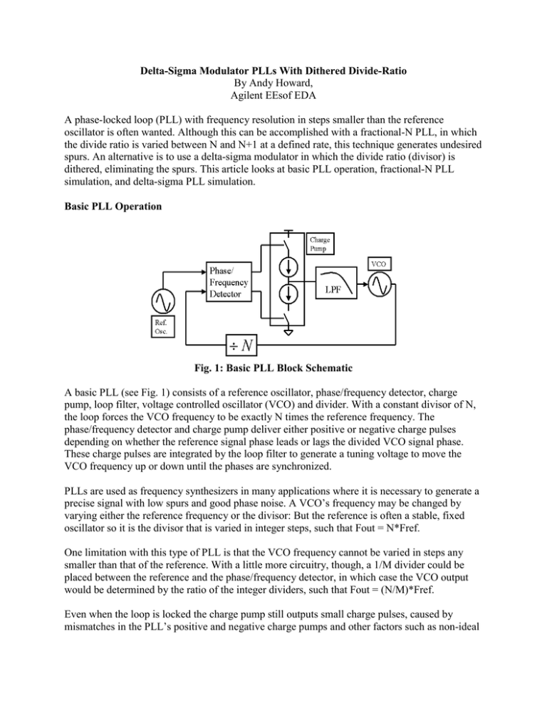
Delta-Sigma Modulator PLLs With Dithered Divide-Ratio By Andy Howard, Agilent EEsof EDA A phase-locked loop (PLL) with frequency resolution in steps smaller than the reference oscillator is often wanted. Although this can be accomplished with a fractional-N PLL, in which the divide ratio is varied between N and N+1 at a defined rate, this technique generates undesired spurs. An alternative is to use a delta-sigma modulator in which the divide ratio (divisor) is dithered, eliminating the spurs. This article looks at basic PLL operation, fractional-N PLL simulation, and delta-sigma PLL simulation. Basic PLL Operation Fig. 1: Basic PLL Block Schematic A basic PLL (see Fig. 1) consists of a reference oscillator, phase/frequency detector, charge pump, loop filter, voltage controlled oscillator (VCO) and divider. With a constant divisor of N, the loop forces the VCO frequency to be exactly N times the reference frequency. The phase/frequency detector and charge pump deliver either positive or negative charge pulses depending on whether the reference signal phase leads or lags the divided VCO signal phase. These charge pulses are integrated by the loop filter to generate a tuning voltage to move the VCO frequency up or down until the phases are synchronized. PLLs are used as frequency synthesizers in many applications where it is necessary to generate a precise signal with low spurs and good phase noise. A VCO’s frequency may be changed by varying either the reference frequency or the divisor: But the reference is often a stable, fixed oscillator so it is the divisor that is varied in integer steps, such that Fout = N*Fref. One limitation with this type of PLL is that the VCO frequency cannot be varied in steps any smaller than that of the reference. With a little more circuitry, though, a 1/M divider could be placed between the reference and the phase/frequency detector, in which case the VCO output would be determined by the ratio of the integer dividers, such that Fout = (N/M)*Fref. Even when the loop is locked the charge pump still outputs small charge pulses, caused by mismatches in the PLL’s positive and negative charge pumps and other factors such as non-ideal phase/frequency detection. These pulses create sidebands, or spurs, in the VCO output spectrum at offset frequencies equal to the reference. Dealing with these spurs requires design tradeoffs: For fine frequency resolution we want a low reference frequency, but this will cause spurs to be generated closer to Fout and a tighter loop filter bandwidth is required to filter them. PLLs with tighter loop bandwidths have longer transient settling times (from one frequency to another) and may not operate fast enough. (Ref. [1] has a discussion of PLL settling time requirements.) Also, the narrower the loop bandwidth the less suppression there is of the VCO’s phase noise outside the loop bandwidth. Fractional-N Synthesis To Achieve Finer Frequency Resolution Fractional-N is a popular technique to achieve frequency resolution finer than the reference frequency. In this approach, the divisor is varied periodically between two integer values. Fig. 2: A fractional-N Synthesizer PLL Block Schematic The average VCO frequency of this type of PLL (see Fig. 2) is determined from equation (2) in Ref. [2], which is repeated here: • Average Fvco = [TnNFref + Tn+1(N+1)Fref]/(Tn + Tn+1), which can be reduced to: • Average Fvco = [N + (Tn+1)/(Tn + Tn+1)]*Fref = (N+fraction)*Fref Therefore, the fractional part of the division ratio (divisor) is determined by the duty cycle: The fraction of the time that the divider is dividing by N+1. This type of PLL may be modeled using an accumulator that sums the desired fraction to itself each reference cycle (Ref. [2].) While the accumulator’s sum is less than its total count capacity there is no overflow and the divisor is N. When the accumulator reaches capacity it overflows and the divisor is reset to N+1. If the desired fraction, say, is 0.1 then the accumulator will overflow once every 10th reference cycle. Or if the desired fraction is 0.5 then the overflow will be every other reference cycle. In fractional-N PLLs the inputs to the phase/frequency detector are not at the same frequency as the divided VCO signal is at (1 + fraction/N)*Fref. This frequency difference means that the phase of the VCO advances at a fractional-radian rate faster than a frequency N*Fref and the accumulator sums this at the same rate. An accumulator overflow occurs when the VCO phase difference (relative to the reference) reaches 2π radians and the divisor increases to N+1 for one cycle. This subtracts 2π/N radians from the divided VCO signal and the phases of the inputs to the phase/frequency detector are again equal. A numerical example is given in Ref. [2.] Fractional-N PLL Simulation Fig. 3: A Fractional-N PLL Simulation Set-Up To simulate a fractional-N PLL (see Fig. 3) using Agilent’s EEsof Advanced Design System 2001 (ADS 2001), co-simulation is used to allow numeric processing with traditional simulators that solve Kirchoff’s Laws. On this top-level view various parameters are set, such as the reference frequency, simulation time-step, bit width of the accumulator, nominal divisor, and the fraction -- which is set equal to the constant value that is the input to the accumulator. The five timed-sink components collect data to be displayed after the simulation. Fig. 4: The PLL Sub-Circuit The PLL sub-circuit (see Fig. 4) consists of a behavioral-model phase/frequency detector, a charge pump, a loop filter, a VCO/divide-by-N block and a reference source and is designed with a unity-gain frequency of 6.6 kHz (see Ref. [1] for the choice of phase margin and, therefore, the component values.) The phase/frequency detector model uses dual flip-flops and outputs digital pulses with durations that depend on the phase difference between the inputs. Phase/frequency detectors in actual PLLs are asynchronous, meaning that outputs do not change in response to a clock signal, but only when inputs pass a specific logic threshold. Such circuits are time-consuming to simulate because very fast clock edges (<100 ps) must be captured even though the overall simulation time may be milliseconds. The phase/frequency detector model uses interpolation to determine the input signal transitions with finer resolution than the time step, and actually amplitude-modulates the output signal pulses to overcome the fixed time-step limitation of the simulator (see Ref. [3].) In order to more accurately compute the phase difference between the inputs, the signals used are sawtoothed. The charge pump is modeled as ideal voltage-controlled current sources that source/sink current into/from the loop filter. Non-ideal sources, or transistors, can model nonlinear behavior. The VCO/divide-by-N combination into a single behavioral model achieves a more efficient simulation, making use of the ADS that allow creation or modification of such models just by editing equations on a schematic -- without requiring them to be compiled. When running transient or lock-time simulations (when there is no need to see the VCO signal) this combined model allows the simulation time step to be set just small enough to sample the divided signal. This means simulations can be run with a time step several orders of magnitude larger (and faster!) than would be required to sample the VCO. The block has control voltage and delta divide-by-N inputs, a nominal divisor setting and an equation for characterizing the VCO’s frequency-vs.-tuning voltage. The instantaneous divisor is the sum of the nominal divisor (N = N0) and the voltage at the delta divide-by-N input. In this simulation, this delta divide-by-N input comes from the accumulator’s output -- either 0 or 1. The block has three outputs: The envelope of the VCO signal, its instantaneous frequency, and the phase of the divided signal as a sawtooth wave, varying from -π and + π. The phase of the divided signal is selected as the output rather than a sinusoid because, as described earlier, the phase/frequency detector works most accurately when it compares input sawtooths. Accumulator Modeling Fig. 5: An Accumulator Simulation Accumulators are key in delta-sigma modulators and simulated (see Fig. 5) consist of an adder, two bus rippers and a data register. The accumulator continuously adds a constant (in this case the fraction) to itself. The arithmetical setting of the first bus ripper’s output is 1.0, meaning it outputs a 1 if the adder output is >1, otherwise it outputs a 0: The overflow output. The other bus ripper feeds the fractional part of the adder’s output back to its input. For example, if the desired fraction to be summed is 100÷(210) = 0.09765625 (offset value divided by 2 to the power of the number of delta-sigma bits), then after 10 summations, the adder output will be 1.07421875 (11*0.09765625), the overflow will be 1, and the amount fed back to the input of the adder will be 0.07421875. With this simulation the precision (number of bits used) can easily be changed. Fig. 6: Accumulator Simulation Outputs, Including The Overflow Bit The sawtooth waveform of the accumulator output and the overflow bit switch (see Fig. 6) from 0 to 1 about once every 10 times a summation occurs and the Schmidt trigger block (Fig. 3, again) samples the clock sawtooth waveform and outputs a logic 1, once per divided VCO cycle. This causes the accumulator overflow output to be sampled once every clock cycle. Fractional-N Co-Simulation Results Fig. 7: VCO Output Spectrum The spurs generated by this fractional-N PLL can clearly be seen (Fig. 7.) The signal is at (N0+fraction)*Fref, with high spurs at offset frequencies equal to multiples of fraction*Fref. Fig. 8: VCO Output Signal Frequency Error Vs. Time The frequency error plot shows (Fig. 8) how the frequency deviates periodically around its nominal value. Using A Delta-Sigma Modulator To Eliminate Spurs Ideally the divisor would be continuously variable, set arbitrarily, which would attain continuous frequency resolution, without spurs. Of course this is not possible because the divider must be set to integer values. In the fractional-N PLL, the desired fraction is converted by the accumulator to a sequence of 1s and 0s -- with overflow -- which could be considered a coarse, 1-bit ADC. Fig. 9: Block Diagram Of A Simple Delta-Sigma Modulator As described in Refs. [2] and [4], an accumulator may be considered to be a simple delta-sigma modulator (see Fig. 9) where the 1/(1-z-1) block implements the basic accumulator operation. The 1-bit quantizer outputs a 0, or a 1 when it overflows. The overflow is subtracted from the input, in effect keeping the fractional part of the accumulated sum in the accumulator. The output signal (the accumulator overflow) in the Z-domain (sampled data, frequency domain) is represented by: • Y(z) = F(z) + (1-z-1)*Eq(z) If the input signal was varying randomly, then the quantization error would also vary randomly and the quantization noise would be high-pass filtered. To do this, set z = ejω; at low frequencies: ( − jω ) 2 • 1 − e − jω ≈ 1 − (1 − jω + + ...) ≈ jω , which is close to 0. 2! Alternatively: • e − jω = cos ω − j sin ω , so for ω small, the modulus is: • | 1 − e − jω |≈| j sin ω | The phase noise (spurs) would also be shifted further from the VCO center frequency. This is not so in a fractional-N synthesizer where the input signal is constant and quantization noise increases periodically (at overflow) so the output spectrum has large, undesired sidebands. Using A Multistage Delta-Sigma Modulator Architecture Fig. 10: Block Diagram For A Multi-Stage Delta-Sigma Modulator In order to attain a divisor with quantization noise that has a high-pass-shaped response, and which does not suffer from the periodicity and spurs of a single-accumulator delta-sigma modulator, a multi-stage architecture can be simulated (Fig. 10) as described in Refs. [2] and [4]. The output frequency of a PLL using a 3-stage modulator is: • Fout(z) = N.F(z)*Fref + (1-z-1)3*Fref*Eq3(z), where Eq3(z) is the quantization noise of the third modulator stage. This equation may be derived easily from the block diagram. This equation gives frequency noise, but phase noise is of more interest in frequency synthesis applications. An equation for the phase noise as a function of offset frequency, f, and the number of modulator stages, m, due to the shaping of the quantization noise is equation (12) in Ref. [2.] However, this does not predict the overall noise performance of the PLL, which also depends on the loop bandwidth, the free-running VCO phase noise, noise from the phase detector and divider, plus other contributing factors. Fig. 11: Three-Stage Delta-Sigma Modulator Simulated In ADS A three-stage delta-sigma modulator can be implemented (Fig. 11) with accumulators and differentiators. The accumulators have a clock input, an input that is accumulated, an overflow output (1 or 0), and an output that is the fractional part of the accumulator’s sum. Fig. 12: Differentiator Sub-Circuit Used In The Delta-Sigma Modulator In the differentiator (Fig. 12) the Port 2 input is differentiated via the data register and the adder, configured to subtract A-B: The current value at Port 2 minus the value one clock sample before. The result is added to Port 3’s ovf, so the sub-circuit combines differentiation with addition. Fig. 13: Multi-Stage Delta-Sigma Modulator PLL in ADS Co-Simulation The delta-sigma modulator allows easy changes to the number of stages or the precision of the arithmetic to view the resulting spectrum. The set-up (Fig. 13) is quite similar to that for fractional-N, and configuring the delta-sigma modulator with a single stage should give the same results. Fig. 14: Simulated Output (Deviation in Divisor) From Modulator; Time And Frequency The simulated output signal (Fig. 14), when added to the nominal divisor, becomes the instantaneous divisor. Note that its spectrum has a high-pass shape, as expected. Fig. 15: Simulated Synthesizer Spectrum And Log-Offset Plot With Close-In Spectrum The simulated output spectrum and a log-offset spectral plot (Fig. 15) show the close-in spectrum. The loop bandwidth has been increased to about 20 kHz and the noise spectrum flattens out above this offset frequency. In the VCO Spectrum plot it should be noted that the Xaxis is not the absolute frequency, but the offset from the nominal analysis frequency at N0*ReferenceFreq. The fraction (in Fig. 13, again) is set to 501÷(210), and this value multiplied by the reference frequency at 1.728 MHz is 845.4375 kHz, which is how far above the nominal analysis frequency the VCO is…as expected. Summary This article shows how to simulate a PLL, using a delta-sigma modulator to achieve a spuriousfree output and very high frequency resolution, with Agilent’s EEsof Advanced Design System 2001. This simulation uses ADS 2001 Circuit Envelope & Agilent Ptolemy simulators as well as ADS's co-simulation technology, for simulating both logic-level functions (like accumulators and differentiators) as well as circuit-level components like Rs, Cs, and behavioral models. Although not shown in this article, transistor-level sub-circuits may be used to replace the behavioral models. The ADS 2001 example file used in this article (PLL_SigmaDelta_prj.zap) can be downloaded at http://www.agilent.com/eesof-eda. References [1] Franceschino, Albert, “Phase-Locked Loop Primer and Application to Digital European Cordless Phone,” Applied Microwaves and Wireless, Fall 1994. [2] Miller, Brian, “Technique Enhances the Performance of PLL Synthesizers,” Microwaves and RF, January 1993. [3] Agilent Technologies, “Phase-Locked Loop Simulation Using Circuit Envelope,” a video available from Agilent EEsof product marketing. [4] Miller, Brian and Robert J. Conley, “A Multiple Modulator Fractional Divider,” IEEE Transactions on Instrumentation and Measurement, Vol. 40, No. 3, June 1991.
