APPLICATION NOTE
®
TD310 USED IN A VOLTAGE QUADRUPLER
by R. LIOU
INTRODUCTION
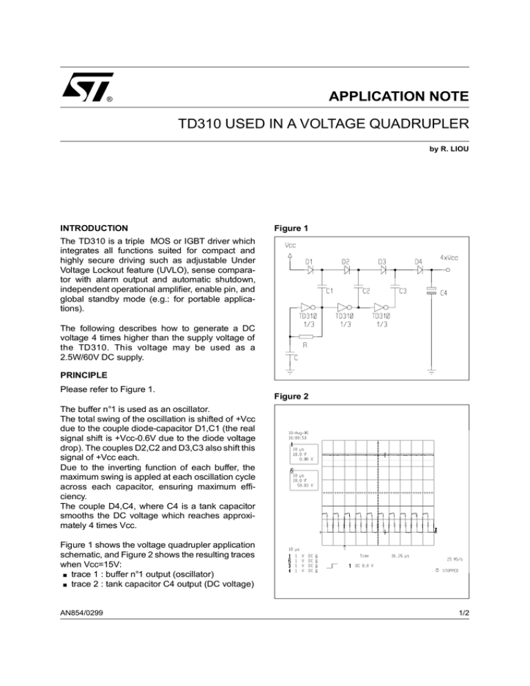
Figure 1
The TD310 is a triple MOS or IGBT driver which
integrates all functions suited for compact and
highly secure driving such as adjustable Under
Voltage Lockout feature (UVLO), sense comparator with alarm output and automatic shutdown,
independent operational amplifier, enable pin, and
global standby mode (e.g.: for portable applications).
The following describes how to generate a DC
voltage 4 times higher than the supply voltage of
the TD310. This voltage may be used as a
2.5W/60V DC supply.
PRINCIPLE
Please refer to Figure 1.
Figure 2
The buffer n°1 is used as an oscillator.
The total swing of the oscillation is shifted of +Vcc
due to the couple diode-capacitor D1,C1 (the real
signal shift is +Vcc-0.6V due to the diode voltage
drop). The couples D2,C2 and D3,C3 also shift this
signal of +Vcc each.
Due to the inverting function of each buffer, the
maximum swing is appled at each oscillation cycle
across each capacitor, ensuring maximum efficiency.
The couple D4,C4, where C4 is a tank capacitor
smooths the DC voltage which reaches approximately 4 times Vcc.
Figure 1 shows the voltage quadrupler application
schematic, and Figure 2 shows the resulting traces
when Vcc=15V:
trace 1 : buffer n°1 output (oscillator)
trace 2 : tank capacitor C4 output (DC voltage)
..
AN854/0299
1/2
APPLICATION NOTE
.
DESIGN CONSIDERATIONS
To each triplet of capacitors C1, C2, C3 corresponds an optimal frequency of oscillation of the
buffer 1.
The traces shown on Figure 2 have been realised
with C1=C2=C3=1µF, at Vcc=15V and 100kHz.
Best efficiency is obtained with 50% oscillator duty
cycle
The voltage across the tank capacitor C4 cannot
exceed 4xVcc - 4xVd (diode voltage drop)
U2/R = 522/103 = 2.7W
NOTES
As the TD310 can be supplied under a very wide
supply voltage range, a 20V supply is achievable
from a 5V supply.
The enable pin and standby mode are still available, as well as a comparator and an operational
amplifier (eg: post regulation).
The same principle, using only two inverters can be
used to make an NxVcc DC voltage supply.
Figure 3 shows the voltage drop across the tank
capacitor C4 (10µF) when a 1kW load is connected. The power dissipated in the load is:
Figure 3
Information furnished is believed to be accurate and reliable. However, STMicroelectronics assumes no responsibility for the
consequences of use of such information nor for any infringement of patents or other rights of third parties which may result from
its use. No license is granted by implication or otherwise under any patent or patent rights of STMicroelectronics. Specifications
mentioned in this publication are subject to change without notice. This publication supersedes and replaces all information
previously supplied. STMicroelectronics products are not authorized for use as critical components in life support devices or systems
without express written approval of STMicroelectronics.
© The ST logo is a trademark of STMicroelectronics
© 1999 STMicroelectronics – Printed in Italy – All Rights Reserved
STMicroelectronics GROUP OF COMPANIES
Australia - Brazil - Canada - China - France - Germany - Italy - Japan - Korea - Malaysia - Malta - Mexico - Morocco
The Netherlands - Singapore - Spain - Sweden - Switzerland - Taiwan - Thailand - United Kingdom - U.S.A.
© http://www.st.com
2/2


