Plasmonics: Merging Photonics and Electronics at Nanoscale
advertisement
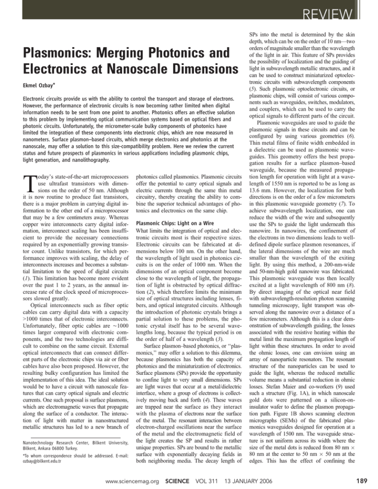
REVIEW Plasmonics: Merging Photonics and Electronics at Nanoscale Dimensions Ekmel Ozbay* Electronic circuits provide us with the ability to control the transport and storage of electrons. However, the performance of electronic circuits is now becoming rather limited when digital information needs to be sent from one point to another. Photonics offers an effective solution to this problem by implementing optical communication systems based on optical fibers and photonic circuits. Unfortunately, the micrometer-scale bulky components of photonics have limited the integration of these components into electronic chips, which are now measured in nanometers. Surface plasmon–based circuits, which merge electronics and photonics at the nanoscale, may offer a solution to this size-compatibility problem. Here we review the current status and future prospects of plasmonics in various applications including plasmonic chips, light generation, and nanolithography. oday_s state-of-the-art microprocessors use ultrafast transistors with dimensions on the order of 50 nm. Although it is now routine to produce fast transistors, there is a major problem in carrying digital information to the other end of a microprocessor that may be a few centimeters away. Whereas copper wire interconnects carry digital information, interconnect scaling has been insufficient to provide the necessary connections required by an exponentially growing transistor count. Unlike transistors, for which performance improves with scaling, the delay of interconnects increases and becomes a substantial limitation to the speed of digital circuits (1). This limitation has become more evident over the past 1 to 2 years, as the annual increase rate of the clock speed of microprocessors slowed greatly. Optical interconnects such as fiber optic cables can carry digital data with a capacity 91000 times that of electronic interconnects. Unfortunately, fiber optic cables are È1000 times larger compared with electronic components, and the two technologies are difficult to combine on the same circuit. External optical interconnects that can connect different parts of the electronic chips via air or fiber cables have also been proposed. However, the resulting bulky configuration has limited the implementation of this idea. The ideal solution would be to have a circuit with nanoscale features that can carry optical signals and electric currents. One such proposal is surface plasmons, which are electromagnetic waves that propagate along the surface of a conductor. The interaction of light with matter in nanostructured metallic structures has led to a new branch of T Nanotechnology Research Center, Bilkent University, Bilkent, Ankara 06800 Turkey. *To whom correspondence should be addressed. E-mail: ozbay@bilkent.edu.tr photonics called plasmonics. Plasmonic circuits offer the potential to carry optical signals and electric currents through the same thin metal circuitry, thereby creating the ability to combine the superior technical advantages of photonics and electronics on the same chip. Plasmonic Chips: Light on a Wire What limits the integration of optical and electronic circuits most is their respective sizes. Electronic circuits can be fabricated at dimensions below 100 nm. On the other hand, the wavelength of light used in photonics circuits is on the order of 1000 nm. When the dimensions of an optical component become close to the wavelength of light, the propagation of light is obstructed by optical diffraction (2), which therefore limits the minimum size of optical structures including lenses, fibers, and optical integrated circuits. Although the introduction of photonic crystals brings a partial solution to these problems, the photonic crystal itself has to be several wavelengths long, because the typical period is on the order of half of a wavelength (3). Surface plasmon–based photonics, or ‘‘plasmonics,’’ may offer a solution to this dilemma, because plasmonics has both the capacity of photonics and the miniaturization of electronics. Surface plasmons (SPs) provide the opportunity to confine light to very small dimensions. SPs are light waves that occur at a metal/dielectric interface, where a group of electrons is collectively moving back and forth (4). These waves are trapped near the surface as they interact with the plasma of electrons near the surface of the metal. The resonant interaction between electron-charged oscillations near the surface of the metal and the electromagnetic field of the light creates the SP and results in rather unique properties. SPs are bound to the metallic surface with exponentially decaying fields in both neighboring media. The decay length of www.sciencemag.org SCIENCE VOL 311 SPs into the metal is determined by the skin depth, which can be on the order of 10 nm—two orders of magnitude smaller than the wavelength of the light in air. This feature of SPs provides the possibility of localization and the guiding of light in subwavelength metallic structures, and it can be used to construct miniaturized optoelectronic circuits with subwavelength components (5). Such plasmonic optoelectronic circuits, or plasmonic chips, will consist of various components such as waveguides, switches, modulators, and couplers, which can be used to carry the optical signals to different parts of the circuit. Plasmonic waveguides are used to guide the plasmonic signals in these circuits and can be configured by using various geometries (6). Thin metal films of finite width embedded in a dielectric can be used as plasmonic waveguides. This geometry offers the best propagation results for a surface plasmon–based waveguide, because the measured propagation length for operation with light at a wavelength of 1550 nm is reported to be as long as 13.6 mm. However, the localization for both directions is on the order of a few micrometers in this plasmonic waveguide geometry (7). To achieve subwavelength localization, one can reduce the width of the wire and subsequently use the SPs to guide the light underneath this nanowire. In nanowires, the confinement of the electrons in two dimensions leads to welldefined dipole surface plasmon resonances, if the lateral dimensions of the wire are much smaller than the wavelength of the exiting light. By using this method, a 200-nm-wide and 50-nm-high gold nanowire was fabricated. This plasmonic waveguide was then locally excited at a light wavelength of 800 nm (8). By direct imaging of the optical near field with subwavelength-resolution photon scanning tunneling microscopy, light transport was observed along the nanowire over a distance of a few micrometers. Although this is a clear demonstration of subwavelength guiding, the losses associated with the resistive heating within the metal limit the maximum propagation length of light within these structures. In order to avoid the ohmic losses, one can envision using an array of nanoparticle resonators. The resonant structure of the nanoparticles can be used to guide the light, whereas the reduced metallic volume means a substantial reduction in ohmic losses. Stefan Maier and co-workers (9) used such a structure (Fig. 1A), in which nanoscale gold dots were patterned on a silicon-oninsulator wafer to define the plasmon propagation path. Figure 1B shows scanning electron micrographs (SEMs) of the fabricated plasmonics waveguides designed for operation at a wavelength of 1500 nm. The waveguide structure is not uniform across its width where the size of the metal dots is reduced from 80 nm 80 nm at the center to 50 nm 50 nm at the edges. This has the effect of confining the 13 JANUARY 2006 189 REVIEW obviously too short for any application of these plasmonic structures. The propagation distance performance of the V groove–shaped SP waveguides has been recently extended to 250 mm (11). By using focused ion-beam milling techniques, 460-mm-long V groove–shaped plasmonic waveguides were fabricated on gold layers that were deposited on a substrate of fused silica. Scanning near-field optical microscope measurements of these structures were made at optical communication wavelengths (1425 to 1620 nm). For a structure with a 0.6-mm-wide and 1.0-mm-deep groove wedge (corresponding to a È17- wedge angle), the SP propagation lengths were measured to be within 90 to 250 mm. The mode was well confined along the lateral direction, and the measured mode width was 1.1 mm. Thus there is a basic trade-off in all plasmon waveguide geometries between mode size and propagation loss. One can have a low propagation loss at the expense of a large mode size, or a high propagation loss with highly confined light. A hybrid approach, where both plasmonic and dielectric waveguides are used, has been suggested as a solution to this tradeoff (12). These waveguides are designed for 1500-nm operation and exhibit losses on the order of –1.2 dB/mm, and they can guide light around 0.5-mm bends. Light can also be efficiently coupled between more conventional silicon waveguides, where these plasmon waveguides with compact couplers and surface plasmon optical devices can be constructed by using planar circuit fabrication techniques. Introducing gain to the plasmonic waveguides can also bring a solution to the limited propagation distances. This situation is theoretically investigated by considering the propagation of SPs on metallic waveguides adjacent to a gain medium (13). The analytic analysis and numeric simulation results show that the gain Fig. 1. (A) FDTD simulations show the electric field medium assists the SP propagation by produced within the plasmon waveguide structure. (B) A compensating for the metal losses, plasmon waveguide consists of nanoscale gold dots on a making it possible to propagate SPs with little or no loss on metal boundaries and silicon-on-insulator surface. [Adapted from (9)] energy more intently to the middle of the guide (Fig. 1A). This structure has been shown to have a decay length longer than 50 mm, whereas theoretical simulations predict a decay length in the order of 500 mm. Figure 1A shows that although the localization along the x direction is subwavelength, the localization extends a few periods along the y direction, which corresponds to localization on the order of a wavelength. Therefore, the subwavelength localization of SPs is limited only to the x direction. To achieve localization in both directions, a new type of highly localized plasmon has been analyzed and experimentally demonstrated in metals with V-shaped grooves (10). The major features of plasmons in V grooves include a combination of strong localization, single-mode operation, the possibility of nearly 100% transmission through sharp bends, and a high tolerance to structural imperfections. For the localization and guiding to occur, the wedge angle (q) of the V groove should be smaller than a critical angle. For V grooves made from silver with a vacuum wavelength of 0.6328 mm, this critical wedge angle is found to be 102-. The measured lateral localization of a structure with a 40- wedge angle is È300 nm, which is superior to the nanoparticle-based plasmonic waveguides. However, the reported experimental and theoretical decay lengths for the same V groove–shaped plasmonic waveguide are 1.5 mm and 2.25 mm, respectively, which are Fig. 2. (A) SEM image of a nanodot focusing array coupled to a 250-nm-wide Ag strip guide. (B) NSOM image of the SP intensity showing subwavelength focusing. [Adapted from (15)] 190 13 JANUARY 2006 VOL 311 SCIENCE guides. The calculated gain requirements suggest that lossless, gain-assisted surface plasmon propagation can be achieved in practice for infrared wavelengths. Recently, a new kind of SP geometry has been suggested to solve theoretically the issue of confinement versus propagation length (14). The new mechanism for confining much more field in the low-index region rather than in the adjacent high-index region is based on the relative dispersive characteristics of different surface plasmon modes that are present in these structures. The structures have a subwavelength modal size and very slow group velocity over an unusually large frequency bandwidth. Simulations show that the structures exhibit absorption losses limited only by the intrinsic loss of the metal. Currently, there is no experimental data that supports these simulations. However, the new suggested SP structure is quite promising and deserves attention from the experimental research groups that are working on plasmonic waveguides. Plasmonic chips will have optical input and output ports, and these ports will be optically connected to conventional diffraction-limited photonic devices by plasmonic couplers (8). The couplers should have high conversion efficiency, along with a transmission length that is longer than the optical wavelength to avoid the direct coupling of the propagating far-field light to the nanophotonic devices inside the plasmonic chip. A promising candidate for this feature can be fabricated by combining hemispherical metallic nanoparticles that work as a plasmonic condenser and a nanodot-based plasmonic waveguide (15). When the focused plasmons move into the coupler, the transmission length through the coupler is 4.0 mm. Nanodots can also be used for focusing SPs into a spot of high near-field intensity having a subwavelength width (16). Figure 2A shows the SEM image of such a sample containing 19 200-nm through-holes arranged on a quarter circle with a 5-mm radius. The SPs originating from these nanodots are coupled to a metal nanostrip waveguide. A near-field scanning optical microscopy (NSOM) image of this structure was taken at 532-nm incident wavelength with horizontal polarization. The near-field image (Fig. 2B) shows that the focused SPs propagate along the subwavelength metal guide, where they partially penetrate into the 100-nm-wide bifurcation at the end of the guide, thus overcoming the diffraction limit of conventional optics. The measured propagation distance is limited to 2 mm, and the propagation distances are expected to be much longer with improved fabrication processes and by using properly designed metal-dielectric hybrid structures. The combination of focusing arrays and nanowaveguides may serve as a basic element in planar plasmonic circuits. Active control of plasmons is needed to achieve plasmonic modulators and switches. www.sciencemag.org REVIEW Plasmonic signals in a metal-on-dielectric waveguide containing a gallium section a few microns long can be effectively controlled by switching the structural phase of gallium (17). The switching can be achieved by either changing the waveguide temperature or by external optical excitation. The signal modulation depth can exceed 80%, and switching times are expected to be in the picosecond time scale. The realization of an active plasmonic device by combining thin polymer films containing molecular chromophores with thin silver film has also been reported (18). The molecular plasmonic device consists of two polymer layers, one containing donor chromophore molecules and the other containing acceptor fluorophore molecules. Coupled SPs are shown to provide an effective transfer of excitation energy from donor molecules to acceptor molecules on opposite sides of metal film up to 120 nanometers thick. The donors absorb incident light and transfer this excitation energy by dipole-dipole interactions to the acceptors. The acceptors then emit their characteristic fluorescence. These results are preliminary demonstrations for active control of plasmonic propagation, and future research should focus on the investigation of electro-optic, all-optical, and piezoelectric modulation of subwavelength plasmon waveguide transmission. Extensive research efforts are being put forth in order to achieve an all-plasmonic chip. In the near term, plasmonic interconnects may be used to address the capacity problem in digital circuits including microprocessors. Conventional electronic interconnects may be used to transfer the digital data among the local arrays of electronic transistors. But, when a lot of data need to travel from one section of a chip to another remote section of the chip, electronic information could be converted to plasmonic information, sent along a plasmonic wire, and converted back to electronic information at the destination. Unfortunately, the current performance of plasmonic waveguides is insufficient for this kind of application, and there is an urgent need for more work in this area. If plasmonic components can be successfully implemented as digital highways into electronic circuits, this will be one of the ‘‘killer applications’’ of plasmonics. Plasmonic Light Sources The emerging field of plasmonics is not only limited to the propagation of light in structures with subwavelength dimensions. Plasmonics can also help to generate and manipulate electromagnetic radiation in various wavelengths from optics to microwaves. Since their introduction by Nakamura in 1995 (19), InGaN-based semiconductor light emitting diodes (LEDs) have become promising candidates for a variety of solid-state lightning applications (20). However, semiconductor-based LEDs are also notorious for their low light-emission efficiencies. Plasmonics can be used to solve this efficiency problem (21). When InGaN/GaN quantum wells (QWs) are coated by nanometer silver or aluminum films, the resulting SPs increase the density of states and the spontaneous emission rate in the semiconductor. This leads to the enhancement of light emission by SP-QW coupling, which results in large enhancements of internal quantum efficiencies. Time-resolved photoluminescence spectroscopy measurements were used to achieve a 32-fold increase in the spontaneous emission rate of an InGaN/GaN QW at 440 nm (22). This enhancement of the emission rates and intensities results from the efficient energy transfer from electron-hole pair recombination in the QW to electron vibrations of SPs at the metal-coated surface of the semiconductor heterostructure. This QW-SP coupling is expected to lead to a new class of super bright and high-speed LEDs that offer realistic alternatives to conventional fluorescent tubes. Similar promising results were obtained for organic LEDs (OLEDs), which are now becoming popular as digital displays. In an OLED, up to 40% of the power that can be coupled into air is lost due to quenching by SP modes. A periodic microstructure can be used to recover the power that is normally lost to SPs. Using this approach, strong photoluminescence has been reported from a topemitting organic light-emitting structure, where emission takes place through a thin silver film (23). The results indicate that the addition of a nanopatterned dielectric overlayer to the cathode of top-emitting OLEDs should increase light emission from these structures by two orders of magnitude over a similar planar structure. The dielectric layer acts to couple the surface plasmon-polariton modes on the two metal surfaces, whereas its corrugated morphology allows the modes to scatter to light. An OLED using a p-conjugated polymer emissive layer sandwiched between two semitransparent electrodes was also reported (24). One of the electrodes was an optically thin gold film anode, whereas the cathode was in the form of an optically thick aluminum (Al) film with patterned periodic subwavelength two-dimensional (2D) hole array that showed anomalous transmission in the spectral range of the polymer photoluminescence band. At similar current densities, a sevenfold electroluminescence efficiency enhancement was obtained with the patterned Al device compared with a control device based on imperforated Al electrode, demonstrating that the method of patterning the electrodes into 2D hole arrays is efficient for this structure. Plasmonics can also be used to enhance the performance of lasers (25). A metal nano-aperture was fabricated on top of a GaAs vertical cavity surface emitting laser (VCSEL) for subwavelength optical near-field probing. The optical near-field intensity and the signal voltage of nano-aperture VCSELs exhibit record high values because of the lo- www.sciencemag.org SCIENCE VOL 311 calized surface plasmons in metal nanostructures. The enhancement factors of the optical near-field and voltage signal are 1.8 and 2, respectively. Reducing the nano-aperture reduces the optical resolution of the VCSEL probe from 240 nm to 130 nm. These results show that plasmon enhancement will be helpful for realizing high-resolution optical near-field VCSEL probes. SPs also play a key role in the transmission properties of single apertures and the enhanced transmission through subwavelength hole arrays (26, 27). There has been intense controversy on the physical origin of the enhanced transmission in these structures (28). Recent theoretical and experimental analyses suggest that the enhanced transmission can be explained by diffraction assisted by the enhanced fields associated with SPs (29, 30). Although SPs are mostly studied at optical frequencies, they can also be observed at the microwave, millimeter-wave, and THz frequencies (31). By texturing the metallic surface with a subwavelength pattern, we can create SPs that are responsible for enhanced transmission observed at microwave and millimeter wave frequencies for 1D and 2D gratings with subwavelength apertures (32, 33). A subwavelength circular aperture with concentric periodic grooves can be used to obtain enhanced microwave transmission near the surface plasmon resonance frequency (34). These results show that enhanced transmission from a subwavelength circular annular aperture with a grating is assisted by the guided mode of the coaxial waveguide and coupling to the surface plasmons. A 145-fold enhancement factor is obtained with a subwavelength circular annular aperture surrounded by concentric periodic grooves. The same structure also exhibits beaming properties that are similar to the beaming effects observed from a subwavelength aperture at optical wavelengths (35). Figure 3 shows the electromagnetic waves from a subwavelength circular annular aperture surrounded by concentric periodic grooves. The radiated electromagnetic waves have a very strong angular confinement around the surface mode resonance frequency, in which the angular divergence of the beam is T3-. Enhanced transmission at THz wavelengths is also reported for a freestanding metal foil perforated with periodic arrays of subwavelength apertures (36). The peak transmission at the lowest frequency resonance is È0.6 for each aperture array, which is a factor of È5 larger than the fractional area occupied by the apertures. Doped semiconductors exhibit a behavior at THz frequencies similar to that of metals at optical frequencies, thus they constitute an optimal material for THz plasmonics (37). Enhanced transmission of THz radiation is observed by using arrays of subwavelength apertures structured in n-type silicon. This enhancement can be explained by the resonant tunneling of SPs that can be excited at THz wavelengths 13 JANUARY 2006 191 REVIEW Fig. 3. Calculated (A) and measured (B) electric field distribution from a subwavelength circular annular aperture with a grating at the resonance frequency. The measured electric field intensity is confined to a narrow spatial region and propagates without diffracting into a wide angular region, which is in good agreement with the simulations. Fig. 4. The images of an arbitrary object obtained by different methods. (A) FIB image of the object. (B) The image obtained on photoresist with a silver superlens. (C) The image obtained on photoresist with conventional lithography. (D) Comparison of both methods. [Adapted from (40)] in doped semiconductors. The transmission increases markedly as the aperture size is augmented and as the array thickness is reduced. Plasmonic Nanolithography The minimum feature size used within stateof-the-art electronic circuits is on the order of 50 nm, and new lithography techniques need to be developed to fabricate these integrated circuits with nanometer-scale dimensions. Optical projection lithography at shorter optical wavelengths can be used to reach the desired feature sizes. However, the change of the illumination wavelength to shorter wavelengths means new light sources, photoresists, and optics that are becomingly increasingly more complex as the wavelength becomes smaller. SPs result in a strongly enhanced nanoscale spatial distribution of an electrical field near the metal surface. When the resonance frequency 192 falls within the sensitivity range of a photoresist, the resulting enhanced optical field that is close to the metal surface can locally cause increased exposure of a thin layer of resist directly below the mask. Because the technique is not diffraction limited, it can produce subwavelength structures using broad beam illumination of standard photoresist with visible light. Using this technique, sub–100-nm lines have been patterned photolithographically at a wavelength of 436 nm (38). Theoretical simulations of plasmonic nanolithography predict even better performance (39). Finite difference time domain (FDTD) simulations of isolated silver particles on a thin resist layer show that broad beam illumination with p-polarized light at a wavelength of 439 nm can produce features as small as 30 nm, or l/14, where l is the wavelength. Depending on the exposure time, lateral spot sizes ranging from 13 JANUARY 2006 VOL 311 SCIENCE 30 to 80 nm with exposure depths ranging from 12 to 45 nm can be achieved. The performance of plasmonic nanolithography can be boosted by using the ‘‘superlens’’ concept introduced by Pendry (40). A superlens can be used to enhance evanescent waves via the excitation of surface plasmons. The gain obtained from plasmonic excitation inside the superlens compensates for the loss of the evanescent waves outside of the superlens. The reconstructed evanescent waves can then be used to restore an image below the diffraction limit on the other side of the lens. This unusual lens can be constructed by using a thin slab of material with negative permittivity or permeability, or both. By using silver as a natural optical superlens, sub–diffraction-limited imaging with 60 nanometer half-pitch resolution, or one-sixth of the illumination wavelength, was demonstrated (41). By proper design of the working wavelength and the thickness of silver, which allows access to a broad spectrum of subwavelength features, arbitrary nanostructures can also be imaged with good fidelity. Figure 4 compares the performance of this superlens-based plasmonic nanolithography to conventional nanolithography. A 365-nm exposure wavelength was used for both nanolithography experiments. The word ‘‘NANO’’ was printed as a mask by a focused ion beam (FIB) system (Fig. 4A). Figure 4B was obtained with the superlens, and the resulting image on the resist is almost perfect. Figure 4C shows the diffraction limited image obtained from the conventional lithography. Figure 4D numerically compares both methods. Although the resolution achieved by conventional methods is limited to È320 nm, the plasmonic nanolithography method was able to generate an image with Èfour times better resolution. Superresolution imaging using the same method was also reported for a 50-nm-thick planar silver superlens at wavelengths around 365 nm (42). Gratings with periods down to 145 nm can be resolved, which agrees well with the FDTD simulations. These are the preliminary demonstrations of superlens-based plasmonic nanolithography, and additional research for further improvements in subwavelength resolution, aerial coverage, and uniformity is needed. After these improvements, plasmonic nanolithography may be a viable alternative to other nanolithography systems. Future Directions and Challenges The field of plasmonics offers several research opportunities. These include plasmonic chips that function as ultra–low-loss optical interconnects, plasmonic circuits and components that can guide light within ultracompact optically functional devices, nanolithography at deep subwavelength scale, superlenses that enable optical imaging with unprecedented resolution, and new light sources with unprecedented performance. To fulfill the promise offered by plasmonics, more research needs to be done in these areas. Some of the challenges that face www.sciencemag.org REVIEW plasmonics research in the coming years are as follows: (i) demonstrate optical frequency subwavelength metallic wired circuits with a propagation loss that is comparable to conventional optical waveguides; (ii) develop highly efficient plasmonic organic and inorganic LEDs with tunable radiation properties; (iii) achieve active control of plasmonic signals by implementing electro-optic, all-optical, and piezoelectric modulation and gain mechanisms to plasmonic structures; (iv) demonstrate 2D plasmonic optical components, including lenses and grating couplers, that can couple single mode fiber directly to plasmonic circuits; and (v) develop deep subwavelength plasmonic nanolithography over large surfaces. Conclusion The research on plasmonics has made major advances in the past few years. Besides creating new photonics devices, which are considerably smaller than the propagating light’s wavelength, plasmonics is expected to be the key nanotechnology that will combine electronic and photonic components on the same chip. References and Notes 1. M. J. Kobrinsky et al., Intel Technol. J. 8, 129 (2004). 2. M. Born, E. Wolf, Principles of Optics (Cambridge Univ. Press, Cambridge, 1999). 3. J. D. Joannopoulos, R. D. Meade, J. N. Winn, Photonic Crystals: Molding the Flow of Light (Princeton Univ. Press, Princeton, 1995). 4. H. Raether, Surface Plasmons (Springer, Berlin, 1988). 5. W. L. Barnes, A. Dereux, T. W. Ebbesen, Nature 424, 824 (2003). 6. S. A. Maier, H. A. Atwater, J. Appl. Phys. 98, 011101 (2005). 7. P. Berini, R. Charbonneau, N. Lahoud, G. Mattiussi, J. Appl. Phys. 98, 043109 (2005). 8. J. R. Krenn, J. C. Weeber, Philos. Trans. R. Soc. London Ser. A 362, 739 (2004). 9. S. A. Maier, P. E. Barclay, T. J. Johnson, M. D. Friedman, O. Painter, Appl. Phys. Lett. 86, 071103 (2005). 10. D. Pile et al., Appl. Phys. Lett. 87, 061106 (2005). 11. S. I. Bozhevolnyi, V. S. Volkov, E. Devaux, T. W. Ebbesen, Phys. Rev. Lett. 95, 046802 (2005). 12. M. Hochberg, T. Baehr-Jones, C. Walker, A. Scherer, Opt. Exp. 12, 5481 (2004). 13. M. P. Nezhad, K. Tetz, Y. Fainman, Opt. Exp. 12, 4072 (2004). 14. A. Karalis, E. Lidorikis, M. Ibanescu, J. D. Joannopoulos, M. Soljacic, Phys. Rev. Lett. 95, 063901 (2005). 15. W. Nomura, M. Ohtsu, T. Yatsui, Appl. Phys. Lett. 86, 181108 (2005). 16. L. Yin et al., Nano Lett. 5, 1399 (2005). 17. A. V. Krasavin, A. V. Zayats, N. I. Zheludev, J. Opt. Pure Appl. Opt. 7, 85 (2005). 18. P. Andrew, W. L. Barnes, Science 306, 1002 (2004). 19. S. Nakamura, G. Fasol, The Blue Laser Diode: GaN-Based Light Emitting Diode and Lasers (Springer, Berlin, 1997). 20. E. F. Schubert, J. K. Kim, Science 308, 1274 (2005). 21. J. Vuckovic, M. Loncar, A. Scherer, IEEE J. Quant. Electr. 36, 1131 (2000). 22. K. Okamoto et al., Appl. Phys. Lett. 87, 071102 (2005). www.sciencemag.org SCIENCE VOL 311 23. S. Wedge, J. A. E. Wasey, I. Sage, W. L. Barnes, Appl. Phys. Lett. 85, 182 (2004). 24. C. Liu, V. Kamaev, Z. V. Vardenya, Appl. Phys. Lett. 86, 143501 (2005). 25. J. Hashizume, F. Koyama, Opt. Exp. 12, 6391 (2004). 26. T. W. Ebbesen et al., Nature 391, 667 (1998). 27. T. Thio et al., Opt. Lett. 26, 1972 (2004). 28. H. J. Lezec, T. Thio, Opt. Exp. 12, 3629 (2004). 29. J. Pendry, L. Martin-Moreno, F. J. Garcia-Vidal, Science 305, 847 (2004). 30. W. L. Barnes et al., Phys. Rev. Lett. 92, 107401 (2004). 31. A. P. Hibbins, B. R. Evans, J. R. Sambles, Science 308, 670 (2004). 32. S. Akarca-Biyikli, I. Bulu, E. Ozbay, Appl. Phys. Lett. 85, 1098 (2004). 33. M. Beruete et al., Opt. Lett. 12, 3629 (2004). 34. H. Caglayan, I. Bulu, E. Ozbay, Opt. Exp. 13, 1666 (2005). 35. H. J. Lezec et al., Science 297, 820 (2002). 36. H. Cao, A. Nahata, Opt. Exp. 12, 1004 (2004). 37. J. G. Rivas, M. Kuttge, P. H. Bolivar, H. Kurz, Phys. Rev. Lett. 93, 256804 (2005). 38. X. Luoa, T. Ishihara, Appl. Phys. Lett. 84, 4780 (2004). 39. P. G. Kik, S. A. Maier, H. A. Atwater, Phys. Rev. B 69, 045418 (2004). 40. J. B. Pendry, Phys. Rev. Lett. 85, 3966 (2000). 41. N. Fang, H. Lee, C. Sun, X. Zhang, Science 308, 534 (2005). 42. D. O. S. Melville, R. J. Blaikie, Opt. Exp. 13, 2127 (2005). 43. This work was supported by the projects EU–DALHM, EU–NOE–METAMORPHOSE, EU–NOE–PHOREMOST, and TUBITAK-104E090. E.O. also acknowledges partial support from the Turkish Academy of Sciences. 10.1126/science.1114849 13 JANUARY 2006 193
