Digital Controller
for Isolated Power Supply Applications
ADP1043
Preliminary Technical Data
FEATURES
PRODUCT OVERVIEW
Integrates all typical controller functions
Digital control loop
Remote and local voltage sense
Primary and secondary side current sense
PWM control
Synchronous rectifier control
Hot-swap sense and control
Current sharing
Integrated programmable loop filter
I2C interface
Extensive fault detection and protection
Extensive programming
Fast calibration
8 Kb EEPROM
Standalone or microcontroller control
The ADP1043 is a secondary side power supply controller IC
that is designed to provide all the functions that are typically
needed in an isolated ac/dc or dc/dc control application.
APPLICATIONS
A comprehensive GUI is provided for easy design of loop filter
characteristics and programming of the safety features. The
industry-standard I2C bus gives access to the many monitoring
and system test functions.
The ADP1043 is optimized for minimal component count,
maximum flexibility, and minimum design time. Features
include remote voltage sense, local voltage sense, primary and
secondary side current sense, PWM generation, and hot-swap
sense and control. The control loop is digital, with an integrated
programmable digital filter. Protection features include current
limiting, ac sense, UVLO, and OVP (overvoltage protection).
The built-in EEPROM provides extensive programming of the
integrated loop filter, PWM signal timing, inrush current, soft
start timing and sequencing. Reliability is improved through a
built-in checksum and redundancy of critical circuits.
AC/DC power supplies
Isolated dc/dc power supplies
Redundant power supplies
Parallel power supplies
Server, storage, network, and communications infrastructure
www.BDTIC.com/ADI
The ADP1043 is available in a 32-lead LFCSP package and
operates from a single 3.3 V supply.
PFC
AC
INPUT
LOAD
DRIVER
SR1 SR2
DRIVER
ACSNS CS2+ CS2–
PGND
VS1
GATE
VS2
CS1
DRIVER
ADuM1400
OUTA
OUTB
ADP1043
OUTC
OUTD
OUTAUX
RES ADD RTD VCORE FLAGIN PSON PGOOD2 PGOOD1 SDA SCL
VS3+
VS3–
SHAREo
SHAREi
VDD DGND AGND
MICROCONTROLLER
07182-001
VDD
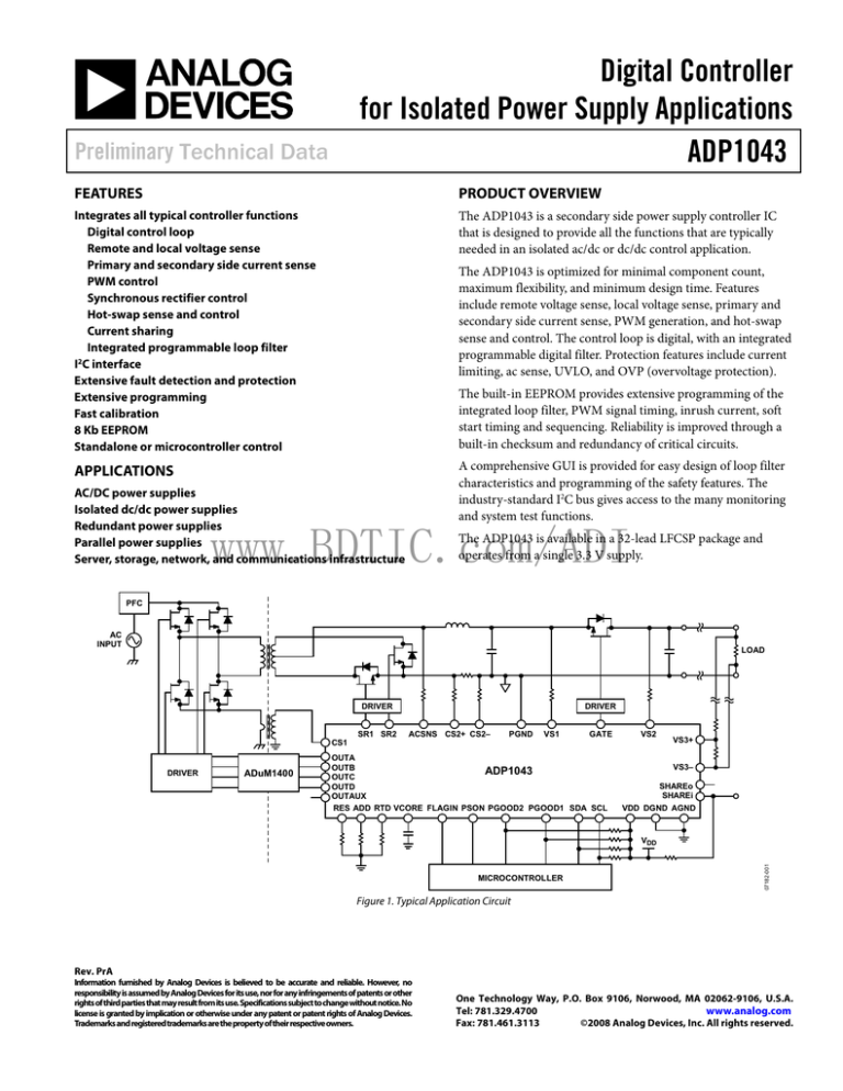
Figure 1. Typical Application Circuit
Rev. PrA
Information furnished by Analog Devices is believed to be accurate and reliable. However, no
responsibility is assumed by Analog Devices for its use, nor for any infringements of patents or other
rights of third parties that may result from its use. Specifications subject to change without notice. No
license is granted by implication or otherwise under any patent or patent rights of Analog Devices.
Trademarks and registered trademarks are the property of their respective owners.
One Technology Way, P.O. Box 9106, Norwood, MA 02062-9106, U.S.A.
Tel: 781.329.4700
www.analog.com
Fax: 781.461.3113
©2008 Analog Devices, Inc. All rights reserved.
ADP1043
Preliminary Technical Data
GENERAL DESCRIPTION
The ADP1043 is a secondary side controller for switch mode
power supplies (SMPS). It is designed for use in isolated redundant
applications. The ADP1043 integrates the typical functions that
are needed to control a power supply. These include
Conventional power supply housekeeping features, such as
remote and local voltage sense and primary and secondary side
current sense, are included. An extensive set of protections is
offered, including overvoltage protection (OVP), overcurrent
protection (OCP), overtemperature protection (OTP),
undervoltage protection (UVP), ground continuity monitoring,
and ac sensing.
Output voltage sense and feedback
Digital loop filter compensation
PWM generation
Current sharing
OrFET control
Current, voltage, and temperature sense
Housekeeping and I2C interface
Calibration and trimming
All these features are programmable through the I2C bus
interface. This bus interface is also used to calibrate the power
supply. Other information, such as input current, output
current, and fault flags, is also available through the digital bus
interface.
The main function of controlling the output voltage is
performed using the feedback ADCs, the digital loop filter, and
the PWM block. The feedback ADCs use a patented multipath
approach. There is a combination of a high speed, low
resolution (fast and coarse) ADC and a low speed, high
resolution (slow and accurate) ADC. Loop compensation is
implemented using the digital filter. This PID (proportional,
integral, derivative) filter is implemented in the digital domain,
allowing easy programming of filter characteristics, which is of
great value in customizing and debugging designs. The PWM
block generates up to six programmable PWM outputs for
control of FET drivers and synchronous rectification FET
drivers. This programmability allows many traditional and
unique switching topologies to be realized.
The internal 1024-byte EEPROM makes it possible to store all
programmed values and allows standalone control without a
microcontroller. Approximately 700 bytes of the EEPROM are
available for user information, such as version and manufacturing date.
The ADP1043 comes with a free downloadable GUI, which
provides all the necessary software to program the part.
GATE
VS1
PGND
ACSNS
CS2+
CS2–
www.BDTIC.com/ADI
The ADP1043 operates from a single 3.3 V supply and is
specified from −40°C to +85°C.
VS2
ADP1043
VREF
OSC
ADC
CS1
ADC
ADC
ADC
ADC
ADC
SR1
SR2
PWM
PWM
ENGINE
DIGITAL
CORE
OUTC
OUTD
OUTAUX
VDD
UVLO
ADC
LDO
VCORE
RES
VS3–
SHAREo
OUTA
OUTB
VS3+
SHAREi
8kB EEPROM
PGOOD1
I2C
INTERFACE
PGOOD2
ADC
FLAGIN
PSON
IREF
SCL
AGND
SDA
DGND
ADD
RTD
Figure 2. Functional Block Diagram
Rev. PrA | Page 2 of 8
07182-002
•
•
•
•
•
•
•
•
A current share bus interface is provided for parallel power
supplies. The part also has hot-swap OrFET sense and control
for N+1 redundant power supplies.
Preliminary Technical Data
ADP1043
32
31
30
29
28
27
26
25
VS3+
VS3–
RES
ADD
RTD
VDD
VCORE
DGND
PIN CONFIGURATION AND FUNCTION DESCRIPTIONS
1
2
3
4
5
6
7
8
PIN 1
INDICATOR
ADP1043
TOP VIEW
(Not to Scale)
24
23
22
21
20
19
18
17
SHAREi
SHAREo
PGOOD1
PGOOD2
FLAGIN
PSON
SDA
SCL
07182-003
SR1
SR2
OUTA
OUTB
OUTC
OUTD
OUTAUX
GATE
9
10
11
12
13
14
15
16
VS2
AGND
VS1
CS2–
CS2+
ACSNS
CS1
PGND
Figure 3. Pin Configuration
Table 1. Pin Function Descriptions
Pin No.
1
Mnemonic
VS2
2
AGND
3
VS1
4
CS2−
Description
Power Supply Output Sense Input. This signal is referred to PGND. Input to a low
frequency Σ-Δ ADC. Nominal voltage at this pin should be 1 V.
Analog Ground. This pin is the ground for the analog circuitry of the ADP1043. Star
connect to DGND.
Local Voltage Sense Input. This signal is referred to PGND. Input to a high frequency Σ-Δ
ADC. Nominal voltage at this pin should be 1 V.
Inverting Differential Current Sense Input. Nominal voltage at this pin should be 1 V for
best operation. When using high-side current sense in a 12 V application, a 110 kΩ
resistor should be placed between the sense resistor and this pin. When using low-side
current sense, a 10 kΩ resistor should be placed between the sense resistor and this pin.
When using high-side, use the formula R = (VCOMMONMODE − 1)/100 μA.
Noninverting Differential Current Sense Input. Nominal voltage at this pin should be 1 V
for best operation. When using high-side current sense in a 12 V application, a 110 kΩ
resistor should be placed between the sense resistor and this pin. When using low-side
current sense, a 10 kΩ resistor should be placed between the sense resistor and this pin.
When using high-side, use the formula R = (VCOMMONMODE − 1)/100 μA.
AC Sense Input. This input is connected upstream of the main inductor through a
resistor divider network. The nominal voltage at this pin should be 1 V. This signal is
referred to PGND.
Primary Side Differential Current Sense Input. This is the current transformer input to
measure and control the primary side current. This signal is referred to PGND.
Power Ground. This pin is the ground connection for the main power rail of the power
supply. Star connect to AGND.
Synchronous Rectifier Output. This PWM output is connected to the input of a FET driver.
This pin can be disabled when not in use. This signal is referred to AGND.
Synchronous Rectifier Output. This PWM output is connected to the input of a FET driver.
This pin can be disabled when not in use. This signal is referred to AGND.
PWM Output for Primary Side Switch. This pin can be disabled when not in use. This
signal is referred to AGND.
PWM Output for Primary Side Switch. This pin can be disabled when not in use. This
signal is referred to AGND.
PWM Output for Primary Side Switch. This pin can be disabled when not in use. This
signal is referred to AGND.
PWM Output for Primary Side Switch. This pin can be disabled when not in use. This
signal is referred to AGND.
Auxiliary PWM Output. This pin can be disabled when not in use. This signal is referred
to AGND.
OrFET Gate Drive Output. This output is open drain. This signal is referred to AGND.
www.BDTIC.com/ADI
5
CS2+
6
ACSNS
7
CS1
8
PGND
9
SR1
10
SR2
11
OUTA
12
OUTB
13
OUTC
14
OUTD
15
OUTAUX
16
GATE
Rev. PrA | Page 3 of 8
ADP1043
Preliminary Technical Data
Pin No.
17
18
19
20
21
Mnemonic
SCL
SDA
PSON
FLAGIN
PGOOD2
22
PGOOD1
23
SHAREo
24
SHAREi
25
DGND
26
27
28
VCORE
VDD
RTD
29
ADD
30
RES
31
32
VS3−
VS3+
Description
I2C Serial Clock Input. This signal is referred to AGND.
I2C Serial Data Input and Output (Open Drain). This signal is referred to AGND.
Power Supply On Input. This signal is referred to DGND.
Flag Input. An external signal can be input here to generate a flag condition.
Power-Good Output (Open Drain). This signal is referred to AGND. This pin is controlled
by the PGOOD2 flag. If any flag is set, this pin toggles.
Power-Good Output (Open Drain). This signal is referred to AGND. This pin is controlled
by the PGOOD flag. If any of the following are out of range, this pin toggles: ACSNS, OCP
CS1, OCP CS2, VS1 OVP, VS2 OVP, or UVP.
Share Bus Output Voltage Pin. When configured as a digital share bus, this pin is a digital
output. When configured as an analog share bus, this pin is an open-drain analog output.
This signal is referred to VS3−.
Analog Share Bus Feedback Pin. This signal is input to an ADC in the ADP1043. This
signal is referred to VS3−.
Digital Ground. This pin is the ground for the digital circuitry of the ADP1043. Star
connect to AGND.
Output of 2.5 V Regulator. Connect a 100 nF capacitor from this point to DGND.
Positive Supply Input. Range is from 3 V to 3.6 V. This signal is referred to AGND.
Thermistor Input. A 10 kΩ or 100 kΩ thermistor is placed from this pin to AGND. This
signal is referred to AGND.
Address Select Input. Connect a resistor from ADD to GND. This signal is referred to
AGND.
Resistor Input. This pin sets up the internal voltage reference for the ADP1043. Connect a
50 kΩ resistor (±1%) from RES to GND. This signal is referred to AGND. Decoupling this
pin to AGND is recommended for noise immunity.
Inverting Remote Voltage Sense Input. There should be a low ohmic contact to AGND.
Noninverting Remote Voltage Sense Input. This signal is referred to VS3−.
www.BDTIC.com/ADI
Rev. PrA | Page 4 of 8
Preliminary Technical Data
ADP1043
OUTLINE DIMENSIONS
0.60 MAX
5.00
BSC SQ
0.60 MAX
25
24
PIN 1
INDICATOR
TOP
VIEW
0.50
BSC
4.75
BSC SQ
0.50
0.40
0.30
12° MAX
1.00
0.85
0.80
PIN 1
INDICATOR
32
1
3.25
3.10 SQ
2.95
EXPOSED
PAD
(BOTTOM VIEW)
17
16
9
8
0.25 MIN
3.50 REF
0.80 MAX
0.65 TYP
0.05 MAX
0.02 NOM
SEATING
PLANE
0.30
0.23
0.18
0.20 REF
COPLANARITY
0.08
COMPLIANT TO JEDEC STANDARDS MO-220-VHHD-2
Figure 4. Mechanical Package Dimensions
www.BDTIC.com/ADI
Rev. PrA | Page 5 of 8
ADP1043
Preliminary Technical Data
NOTES
www.BDTIC.com/ADI
Rev. PrA | Page 6 of 8
Preliminary Technical Data
ADP1043
NOTES
www.BDTIC.com/ADI
Rev. PrA | Page 7 of 8
ADP1043
Preliminary Technical Data
NOTES
www.BDTIC.com/ADI
©2008 Analog Devices, Inc. All rights reserved. Trademarks and
registered trademarks are the property of their respective owners.
PR07182-0-2/08(PrA)
Rev. PrA | Page 8 of 8
