AN-0971
APPLICATION NOTE
One Technology Way • P.O. Box 9106 • Norwood, MA 02062-9106, U.S.A. • Tel: 781.329.4700 • Fax: 781.461.3113 • www.analog.com
Control of Radiated Emissions With isoPower Devices
by Mark Cantrell
INTRODUCTION
iCoupler® digital isolators with integrated isolated power
(isoPower) employ isolated dc-to-dc converters that switch
at frequencies as high as 300 MHz. These high frequencies
typically raise concerns about radiated emissions. PCB layout
and construction is a very important tool for controlling radiated emissions from applications containing these components.
This application note identifies the radiation mechanisms and
offers specific guidance on addressing them.
With proper design choices, these products can easily meet
FCC Part 15, Subpart B, Class A (FCC Class A) emissions
standards, and with care, may even meet FCC Part 15,
Subpart B, Class B (FCC Class B) standards in an unshielded
environment. This application note examines PCB-related EMI
mitigation techniques, including board layout and stack-up
issues. Control of emissions from signal cables and chassis
shielding techniques are outside of the scope of this discussion.
isoPOWER OVERVIEW
The ADuM5xxx product family represents a significant step
forward in isolation technology. Analog Devices, Inc., has
leveraged their experience in microtransformer design to create
chip scale dc-to-dc power converters that are incorporated into
signal isolation products. Power levels of up to one-half watt are
available, which is sufficient to power the secondary side of the
iCoupler as well as to provide power to external components.
OSC
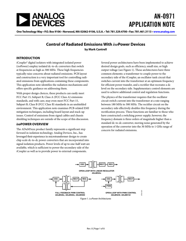
Several power architectures have been implemented to achieve
desired design goals, such as efficiency, small size, or high
output voltage (see Figure 1). These architectures have three
common elements: a transformer to couple power to the
secondary side of the iCoupler, an oscillator tank circuit that
switches current into the transformer at an optimum frequency
for efficient power transfer, and a rectifier that recreates a dc
level on the secondary side. Supplementary control elements are
used to achieve additional control and regulation functions.
The physics of the transformer requires that the oscillator
circuit switch current into the transformer at a rate ranging
between 180 MHz to 300 MHz. The rectifier circuit on the
secondary side effectively doubles this frequency during the
rectification process. These functions are familiar to those who
have constructed a switching power supply; however, the
frequency domain is three orders of magnitude higher than a
standard dc-to-dc converter, moving noise generated by the
operation of the converter into the 30 MHz to 1 GHz range of
concern for radiated emissions.
RECT
REG
OPEN-LOOP WITH LINEAR REGULATOR
ADuM524x
OSC
RECT
REG
OSC
RECT
OPEN-LOOP WITH PWM CONTROL
ADuM5230, ADuM6132
FULL FEEDBACK PWM CONTROL
ADuM540x, ADuM520x, ADuM5000
Figure 1. isoPower Architectures
Rev. 0 | Page 1 of 8
07541-001
PWM
AN-0971
Application Note
TABLE OF CONTENTS
Introduction ...................................................................................... 1 Additional Practices ..........................................................................6 isoPower Overview ........................................................................... 1 Precautions to Meet Isolation Standards ........................................6 Sources of Emissions ........................................................................ 3 Conclusions ........................................................................................7 EMI Mitigation Techniques ............................................................ 4 Rev. 0 | Page 2 of 8
Application Note
AN-0971
SOURCES OF EMISSIONS
There are two sources of emissions in PCBs where isoPower is
used: edge emissions and input-to-output dipole emissions.
•
Cylindrically-radiated magnetic fields coming from
inductive via penetrations radiated out between board
layers eventually meeting the board edge.
•
Strip line image charge currents spreading from high
frequency signal lines routed too close to the edge of
the board.
1
07541-003
Ground and power noise, which is generated by inadequate
bypass of high power current sinks.
8
•
9
Edge emissions occur when unintended currents meet the edges
of ground and power planes. These unintended currents can
originate from:
16
Edge Emissions
Figure 3. Dipole Radiation between Input and Output
Edge emissions are generated (see Figure 2) where differential
noise from many sources meets the edge of the board creating a
dipole. Edge emissions should be predominantly in the plane of
the board.
07541-002
GROUND
POWER
Figure 2. Edge Radiation From a Ground Power Pair
Input-to-Output Dipole Emissions
Input-to-output dipole radiation is generated by driving a
current source across a gap between ground planes. This is the
predominant mechanism for radiation for isoPower applications. Isolated power supplies, by their very nature, drive
current across gaps in ground planes. The inability of high
frequency image charges associated with the power signal to
cross the boundary causes differential signals across the gap
driving the dipole. In many cases, this is a very large dipole as
shown in Figure 3. A similar mechanism causes high frequency
signal lines to radiate when crossing splits in the ground and
power planes. This type of radiation is predominantly
perpendicular to the ground planes.
The ADuM540x device serves as a good example of the issues
involved in generating and mitigating emissions. The oscillator
tank circuit in the ADuM540x runs at approximately 180 MHz.
It can regulate its output to either 5 V or 3.3 V under the control
of a pin on the secondary side. The input voltage can be in the
3 V to 5 V range. The highest power operating mode is 5 V
input and 5 V output. This configuration is examined in this
application note.
When operating under a full 100 mA output load, the average
input current is about 290 mA. This means that the peak
current in the tank circuit is about twice that value at a
switching rate of 180 MHz.
The component’s bypass capacitor is supposed to provide this
high frequency current locally. This is a lot of current for a
bypass capacitor to handle. The capacitor must provide large
charge reserves. At the same time, the capacitor must have a
very low series resistance at 180 MHz. Because this is difficult
to achieve, even with multiple low ESR capacitors near the pins,
the excess noise is injected onto the ground and power planes.
Power is transferred to the output side where it is rectified into
dc. The rectification process doubles the tank frequency to
360 MHz. The input-to-output emissions are predominantly
at the rectification frequency with some contribution from
the tank frequency and higher harmonics. Worst-case data
collected on a 2-layer evaluation board is shown in Figure 4.
Emissions in the near field are shown.
Rev. 0 | Page 3 of 8
AN-0971
line should be installed across the split to allow high frequency
image charges to follow the signal. In isolation applications, this
is not a practical possibility. Adding a high frequency capacitor
between the ground planes does not allow effective high voltage
isolation make it difficult to pass system level isolation
requirements. It would likely be ineffective at 300 MHz and
above due to via and trace inductance.
Many mitigation techniques are available to the designer.
Several techniques that apply directly to the isoPower devices
are identified in this section. The choice of how aggressive
EMI must be addressed for a design to pass FCC emissions
levels depends on the requirements of the design as well as
cost and performance tradeoffs. The easiest radiated EMI
mitigation technique to implement is to place the PCB in a
grounded chassis with filter elements limiting noise escaping
on cable shields. Although this application note does not
discuss this option, note that where PCB related techniques
are not possible, or impractical, this method remains available.
The following techniques are effective in reducing EMI
radiation and on-board noise:
•
Input-to-output ground plane stitching
•
Edge guarding
•
Buried capacitive bypass
•
Power control
Circuit boards with test structures were prepared to evaluate each of these EMI mitigation techniques utilizing the
ADuM540x. The layout of each board was kept as uniform
as possible to allow meaningful comparison of results.
Testing was conducted at an EMI test facility under standard
conditions for FCC Class B certification. As expected, during
EMI testing, it was determined that the emissions at the tank
frequency (180 MHz) were predominantly in the plane of the
board suggesting that the primary mechanism for radiation is
from the PCB edges. The rectification emissions (360 MHz)
are primarily perpendicular to the board suggesting input-tooutput dipole radiation.
Input-to-Output Stitching
The primary cause of radiation across a split in the ground
plane is the lack of a return path for an image charge. In designs
where crossing a split in a reference plane with a high frequency
data line is required, a stitching capacitor paired with the signal
VDDI
VISO
GND1
GNDISO
07541-005
EMI MITIGATION TECHNIQUES
16
A board with near field emissions, as shown in Figure 4, and
without a chassis shield would fail FCC Class B emissions
standards by approximately 40 dB at the 360 MHz peak.
9
Figure 4. Near Field Emissions From a 2-Layer Board
However, a stitching capacitance can be constructed with
copper patterns on the PCB. Figure 5 illustrates a metal pattern
built on a buried power plane. The ground planes, shown in
Figure 5 as dotted outlines, overlap the floating metal structures
creating a very low inductance capacitive bridge between the
GND1 and GNDISO. In actual applications, the ground planes
should have the same outer perimeter as the power planes;
however, they are shown larger to highlight their shape. These
structures should be constructed on inner PCB planes to
preserve the integrity of the clearance distance on the surface
of the PCB. High frequency image charges can now couple to
the secondary side drastically reducing the dipole radiation.
1
HARMONICS AT
540MHz AND
720MHz
8
360MHz
RECTIFIER
07541-004
180MHz
TANK
Application Note
Figure 5. Input-to-Output Capacitive Stitch
When varying amounts of capacitance were added between the
input and output planes, the dipole radiation at 360 MHz and
above was dramatically reduced. Test results for varying
amounts of input-to-output capacitance are shown in Figure 6.
Note that the largest reduction in emissions occurs with a
stitching capacitance of about 100 pF. This is likely because the
capacitance near to the ADuM540x has the greatest effect in
reducing the emissions. Extending the capacitive structures far
from the ADuM540x has less effect. The effect of a 100 pF
stitching structure is a 25 dB decrease in radiated emissions.
The capacitance can be easily estimated with the following
relationship. This equation assumes that the area of overlap
between the floating structure and the ground plane is the same
on each side of the clearance gap of the PCB.
C=
Aε
2d
(1)
where:
C is the coupling capacitance between the input and output sides.
A is the total area of overlap between the buried metal structure
and the local ground planes.
ε is the dielectric constant of the PCB material.
d is the spacing between the ground plane and the buried
structure.
Rev. 0 | Page 4 of 8
Application Note
AN-0971
TANK PEAK EMISSIONS vs. SPANNING CAPACITANCE @ 180MHz
65
RECTIFICATION PEAK vs. STITCHING CAPACITANCE @ 360MHz
90
NO FENCE
2mm FENCE
85
60
EMISSIONS (dB µV/m)
EMISSIONS (dB µV/m)
80
75
70
65
60
55
50
45
0
50
100
150
200
250
300
SPANNING CAPACITANCE (pF)
350
400
40
07541-006
50
0
Figure 6. Emissions vs. Input-to-Output Coupling Capacitance
100
200
CAPACITANCE (pF)
300
400
07541-009
55
Figure 9. Tank Frequency Emissions
Edge Guarding
Buried Capacitance Bypassing
Noise on the power and ground planes that reaches the edge of
a circuit board can radiate as shown in Figure 2. If the edge is
treated with a shield structure, the noise is reflected back into
the interplane space. This can increase the voltage noise on the
planes, but reduces edge radiation.
Buried capacitance bypassing is a technique intended to reduce
the emissions of the board by improving the bypass integrity at
high frequencies. This has two beneficial effects. First, it reduces
the distance that high frequency noise can spread in the ground
and power plane pair. Second, it reduces the initial noise
injected into the power ground planes by providing a bypass
capacitance that is effective between 300 MHz and 1 GHz.
07541-007
GROUND
POWER
GROUND VIA EDGE FENCE
AND GUARD RINGS
Figure 7. Via Fence Structure, Side View
GROUND
FENCE
07541-008
POWER PLANE
Power and ground noise reduction provides a better operating
environment for noise sensitive components near the isoPower
device. Emissions are reduced proportionate to the reduction in
power and ground noise. Although this reduction is not as
significant as that achieved with the stitching or edge guarding
techniques, it significantly improves the power environment of
the board.
The stack-up used for EMI test boards was G-P-S-S-G-S as
shown in Figure 10. A 4 mil core layer was used for the top
power and ground planes. These tightly coupled planes provide
the buried capacitance layer. Having the ground plane on the
top layer allows the isoPower device to couple its ground pins
directly to the copper plane providing the added benefit of good
heat removal from the package.
GROUND
POWER
BURIED
CAPACITIVE
LAYER
SIGNAL
SIGNAL
Figure 8. Via Fence and Guard Ring, Shown on the Power Plane Layer
GROUND
SIGNAL
The edge treatment was expected to have its most pronounced
effect on the edge emissions from the tank circuit at 180 MHz.
Measurements of the tank frequency peak are shown in
Figure 9. This plot shows the reduction of tank frequency
emissions as stitching capacitance is added. The curve is
relatively flat; this confirms that the tank frequency does not
radiate predominantly from the input-to output-dipole.
However, when a 2 mm via fence is added to the same type
of board, the emissions drop by almost 10 dB. This confirms
that edge treatments significantly reduce edge emissions.
07541-009
Making a solid conductive edge treatment on a PCB is possible,
but expensive. A less expensive solution that works well is to
treat the edges of the board with a guard ring structure laced
together by vias. In the ADuM540x test boards, the via spacing
was 2 mm. This structure is shown in Figure 7 and Figure 8.
Figure 10. PCB Stack-Up for Buried Capacitance
Results of testing (see Figure 11) compare VDD noise for three
board stack-ups. The top chart in this figure shows a 2-layer
board without a continuous power plane. The high frequency
noise is very large, approaching 0.5 VP-P. The second chart in
Figure 11 shows a 6-layer stack-up with a common S-G-S-S-P-S
stack-up with about 24 mil of spacing between the ground and
power planes. The noise was reduced by about a factor of four.
The third chart shows a 6-layer stack-up with the buried
Rev. 0 | Page 5 of 8
AN-0971
Application Note
EMISSIONS vs. LOAD @ 360mhZ
capacitance configuration, about 4 mils between power and
ground planes. This reduces the noise to a peak amplitude of
about 60 mV.
60
55
EMISSIONS (dB µV/m)
2-LAYER BOARD NO POWER PLANE
Δ 460mV
50
45
+5V –5V
+3.3V –3.3V
40
6-LAYER BOARD 24mm SPACING POWER-TO-GROUND
Δ 104mV
30
07541-011
6-LAYER BOARD 24mm SPACING POWER-TO-GROUND
Δ 64.0mV
Figure 11. VDD Voltage Noise for Various Stack-Up Options
40
60
80
LOAD CURRENT (mA)
100
120
Figure 13. Emissions at the Rectifier Frequency for
Different Loads and Voltage Configurations
ADDITIONAL PRACTICES
•
All vias in the power path should be as large as practical.
Small vias have high inductance and generate noise. Using
multiple small vias is not as effective in reducing via inductance as a single large via since the bulk of the current goes
through the closest via, even if multiple paths are present.
•
Be very careful to rout signal lines against a single
reference plane. It is vital to maintain the image charge
path so that image charges do not have to travel by
circuitous routs to meet back up with the original signal on
another plane.
•
Do not rout high speed lines close to the edges of the PCB.
•
Routing data or power off-boards, especially through
cables can introduce an additional radiation concern. Feedthrough filter capacitors or similar filter structures can be
used to minimize cable radiation.
In isoPower devices with active feedback or a controllable
PWM control architecture, emissions can be reduced by
keeping the tank circuit off as much as possible. Running
isoPower with light loads achieves this for the ADuM540x.
In addition, devices like the ADuM540x can operate at 3.3 V
input and output. Operation at the lower voltage range reduces
generated noise as well as production of radiated emissions.
Figure 12 and Figure 13 show how emissions at the tank
frequency and the rectification frequency vary with load and
supply voltage, respectively. The tank frequency emissions are
nearly linear with the current load, while the rectification
emissions drop significantly at very light loads. With both light
load and low output voltage, it is possible to reduce tank and
rectification emissions by up to 20 dB.
PRECAUTIONS TO MEET ISOLATION STANDARDS
TANK EMISSIONS vs. LOAD @ 180MHz
70
Most of the techniques discussed in this application note do not
effect board isolation, with the exception of the buried stitching
capacitor. The structure allows coupling of ac transients across
the isolation barrier. In addition, if reinforced insulation is
required across the barrier, then special rules for insulation
thickness and spacing apply.
60
50
40
NO FENCE
2mm FENCE
30
20
10
0
20
40
60
LOAD (mA)
80
100
120
Figure 12. Emissions at the Tank Frequency for Different Load
and Fence Options
07541-012
EMISSIONS (dB µV/m)
20
The following general practices should also be considered:
Power Reduction
0
0
07541-013
35
Special care must be taken when laying out structures for a
buried stitching capacitor across an isolation gap. Insulation in
printed circuit boards does not have any minimum “distance
through the insulation” specification for functional or basic
insulation standards, thus the designer has a great deal of
flexibility in board layout.
If reinforced insulation is required, then a minimum distance
of 0.4 mm (about 16 mil) of insulation along a bonded surface,
such as the gap between copper structures on an internal PCB
layer or directly through the insulation from layer to layer must
be maintained. Although this requirement necessitates careful
Rev. 0 | Page 6 of 8
Application Note
AN-0971
board design, it should not be burdensome if taken into account
at the start of a design.
Capacitive coupling across the isolation barrier allows ac
leakage and transients to couple from one ground plane to the
other. While 100 pF seems small, high voltage high speed
transients can inject significant currents across the barrier
through this capacitance. This must be taken into account if the
application will be subjected to these environments.
CONCLUSIONS
Different EMI mitigation techniques do not interact strongly
with each other. The methods outlined in this application note
address specific radiation sources, and can be combined to
achieve the desired reductions in the associated emissions. Test
boards easily meet FCC Class A standards with no external
shielding by utilizing buried stitching capacitors and edge
fencing. Use of buried decoupling capacitance in the ground
and power planes makes a very quiet environment for precision
measurement applications.
While this application note relies on data collected on the
ADuM540x devices, the techniques are applicable across the
isoPower line. All isoPower couplers contain similar tank and
rectification circuits. The largest currents flow on the primary
side of the devices causing these devices to behave in a similar
manner from a radiated emissions point of view.
Where low ac leakage is required, as in some medical
applications, stitching capacitance may not be a viable solution.
In these applications, grounded metallic chassis enclosures may
be the most practical solution for minimizing emissions.
Rev. 0 | Page 7 of 8
AN-0971
Application Note
NOTES
©2008 Analog Devices, Inc. All rights reserved. Trademarks and
registered trademarks are the property of their respective owners.
AN07541-0-6/08(0)
Rev. 0 | Page 8 of 8


