UXD20P
DC-20 GHz Programmable 1,2,4,8 Binary Prescaler
Features
• Wide Operating Range: DC-20 GHz
• Low SSB Phase Noise: -153 dBc @
10 kHz
• Large Output Swings: 750 mVpp/
side
• Single-Ended and/or Differential
Operation
• Low power consumption: 430 mW
• Size: 4 mm x 4 mm QFN package
• 3 Dividers-in-One with Pass Through
• DC-7 GHz Limit Amp
Application
The UXD20P can be used as a general purpose, fixed modulus prescaler in high frequency PLLs. The low phase noise of the divider
makes it ideal for generating low jitter, synchronous clocks in telecom applications.
Pad Metallization
The QFN package pad metallization consists
of a Ni/Pd/Au plating over a Cu (C194)
leadframe.
Description
The UXD20P is a low noise DC
to 20GHz programmable prescaler
featuring either divide by-1, divide-by-2,
divide-by-4, or divide-by-8 division ratios. In the divide-by-1 mode, the UXD20P is also a DC-7 GHz limit
amplifier. The device features differential
inputs and outputs, adjustable output
swing, and high input sensitivity. The
control inputs are CMOS and LVTTL
compatible. The UXD20P is packaged in
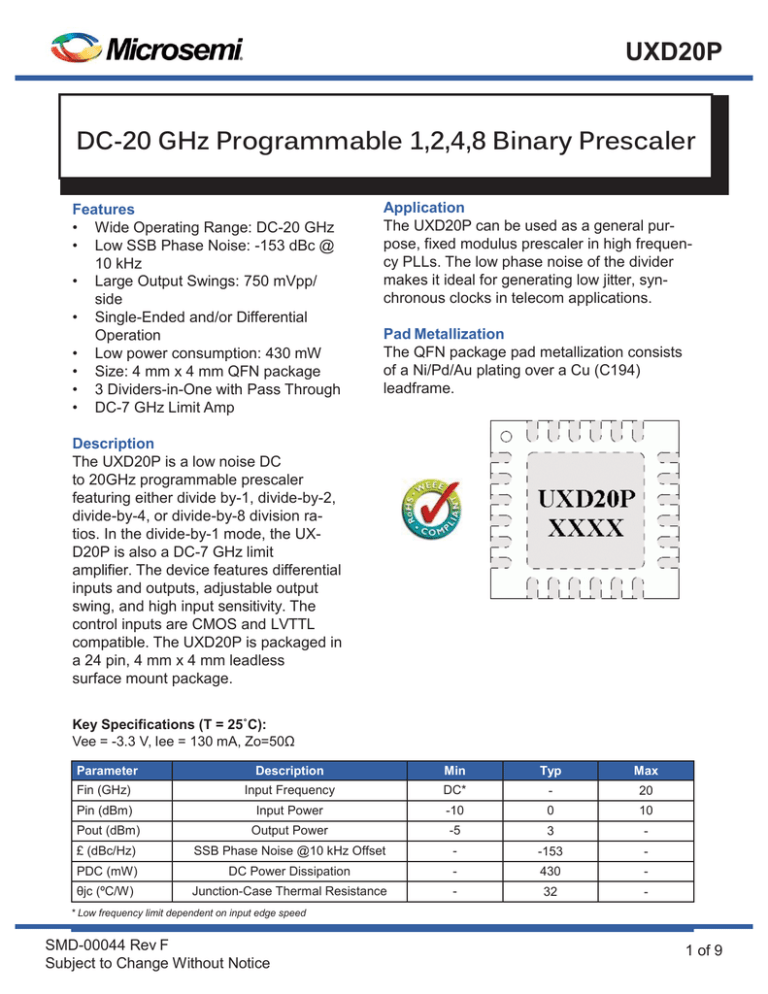
a 24 pin, 4 mm x 4 mm leadless
surface mount package.
Key Specifications (T = 25˚C):
Vee = -3.3 V, Iee = 130 mA, Zo=50Ω
Parameter
Description
Min
Typ
Max
Fin (GHz)
Input Frequency
DC*
-
20
Pin (dBm)
Input Power
-10
0
10
Pout (dBm)
Output Power
-5
3
-
£ (dBc/Hz)
SSB Phase Noise @10 kHz Offset
-
-153
-
PDC (mW)
DC Power Dissipation
-
430
-
θjc (ºC/W)
Junction-Case Thermal Resistance
-
32
-
* Low frequency limit dependent on input edge speed
SMD-00044 Rev F
Subject to Change Without Notice
1 of 9
UXD20P
Frequency Divider Application
Min/Max Single-Ended Input Power
Input Sensitivity Window
Binary Divide-by-2 Output Power,
3rd Harmonic & Input Feedthru
SSB Phase Noise for Binary Divide-by-8 Configuration Input Freq = 7.8 GHz Gain S21
Binary Divide-by-2 Configuration
Input Freq = 20 GHz, 150mV/div
-1V
Binary Divide-by-4 Configuration
Input Freq = 20 GHz, 150mV/div
Binary Divide-by-8 Configuration
Input Freq = 20 GHz, 150mV/div
-1V
SMD-00044 Rev F
Subject to Change Without Notice
-1V
2 of 9
UXD20P
Limit Amplifier Application
S-parameters S21
Pout vs. Frequency
S-parameters S11, S22
S-parameters S12
Group Delay vs. Frequency
Binary Divide-by-1 Configuration
Input Freq = 5 GHz, 150mV/div
-1V
SMD-00044 Rev F
Subject to Change Without Notice
3 of 9
UXD20P
Functional Block Diagram
Table 1: Pin Description
Port Name
Description
Notes
INP
Prescaler Input, Positive Terminal
CML signal levels
INN
Prescaler Input, Negative Terminal
CML signal levels
OUTP
Prescaler Output, Positive Terminal
Requires DC return path to VCC
OUTN
Prescaler Output, Negative Terminal
Requires DC return path to VCC
VADJ
Output Amplitude Control
Tie to VCC via resistor, refer to text for value
SelA
Divider Select Control Line
Divider Select, See Table 1, defaults to logic 0
SelB
Divider Select Control Line
Divider Select, See Table 1, defaults to logic 0
Temp
Temperature Diode
Optional Temperature diode, refer to text
VCC
RF & DC Ground
Positive Supply Voltage
VEE
-3.3 V @ 140 mA
Negative Supply Voltage
Table 2: Divider Mode Select Logic
Simplified Control Logic Schematic
SelA
SelB
Mode
DC Current
0
0
Divide-by-1
105 mA
1
0
Divide-by-8
130 mA
0
1
Divide-by-4
125 mA
1
1
Divide-by-2
120 mA
Table 3: Control Voltages
State
Bias Condition
Comment
Low (logic 0)
VEE @ 0 mA
High (logic 1)
VCC @ 1 mA
Default condition (internally pulled low)
SMD-00044 Rev F
Subject to Change Without Notice
4 of 9
UXD20P
Application Notes
Divider Mode:
The UXD20P supports four division ratios controlled by two select lines which are compatible with
CMOS/LVTTL signaling levels. Table 1 lists the four states for the given logic levels on the SelA and
SelB select lines. For any of the four modes, circuitry which is not used is automatically powered
down to reduce power consumption.
Divider Outputs:
The equivalent circuit of the divider outputs is shown on the below. The outputs require a DC return
path capable of handling ~35 mA per side. If DC coupling is employed, the DC resistance of the
receiving circuits should be ~50 Ω (or less) to VCC to prevent excessive common mode voltage from
saturating the prescaler outputs. If AC coupling is used, the perfect embodiment is shown in figure
2. The discrete R/L/C elements should be resonance free up to the maximum frequency of operation
for broadband applications.
The output amplitude can be adjusted over a 1.5:1 range by one of the two methods The Vadj pin
voltage can be set to VCC for maximum amplituded or VCC-1.3 V for an amplitude ~2/3 the max
swing. Voltages between these two values will produce a linear change in output swing. Alternatively,
users can use a 1k potentiometer or fixed resistor tied between Vadj and VCC. Resistor values approaching 0 ohms will lead to the maximum swing, while values approaching 1k will lead to the minimum output swing. Users who only need/want the maximum swing should simply tie Vadj to VCC.
Equivalent Circuit of Output Buffer
Recommended Circuit for AC Coupled Outputs
Low Frequency Operation:
Low frequency operation is limited by external bypass capacitors and the slew rate of the input clock.
The next paragraph shows the calculations for the bypass capacitors. If DC coupled, the device
operates down to DC for square-wave inputs. Sine-wave inputs are limited to ~50 MHz due to the
10 dBm max input power limitation.
The values of the coupling capacitors for the high-speed inputs and outputs (I/O’s) are determined
by the lowest frequency the IC will be operated at.
C>>
1
2•π•50Ω•flowest
For example to use the device below 30 kHz, coupling capacitors should be larger than 0.1uF.
SMD-00044 Rev F
Subject to Change Without Notice
5 of 9
UXD20P
Diode Voltage vs Temp
for 2 Bias Currents
Temperature Diode:
An optional on chip temperature diode is provided for users
interested in evaluating the IC’s temperature. A single resistor to VCC establishes a nominal current thru the diode.
The voltage developed across the temperature pin (pin 8)
referenced to VEE (pin 9) can then be used to indicate the
surface temperature of the IC. The plot below was obtained
by forcing a fixed current thru the diode for an unbiased
device at multiple temperatures and fitting a line to the data
to allow extrapolation over a range of temperatures.
Package Heatsink:
The package backside provides the primary heat conduction path and should be attached to a
good heatsink on the PC board to maximize performance. User PC boards should maximize the
contact area to the package paddle and contain an array of vias to aid thermal conduction to either
a backside heatsink or internal copper planes.
IC Assembly:
The device is designed to operate with either single-ended or differential inputs. Figures 4, 5 & 6
show the IC assembly diagrams for positive and negative supply voltages. In either case the supply
should be capacitively bypassed to the ground to provide a good AC ground over the frequency range
of interest. The backside of the chip should be connected to a good thermal heat sink.
All RF I/O’s are connected to VCC through on-chip termination resistors. This implies that when VCC
is not DC grounded (as in the case of positive supply), the RF I/O’s should be AC coupled through
series capacitors unless the connecting circuit can generate the correct levels through level shifting.
CML Logic Levels for DC Coupling (T = 25˚C):
Assuming 50 Ω Terminations at Inputs and Outputs
Parameter
Differential
Minimum
Typical
Maximum
{
Logic Inputhigh
Vcc
Vcc
Vcc
Logic Inputlow
Vcc - 0.05 V
Vcc - 0.3 V
Vcc - 1 V
{
Logic Inputhigh
Vcc + 0.05 V
Vcc + 0.3 V
Vcc + 1 V
Logic Inputlow
Vcc - 0.05 V
Vcc - 0.3 V
Vcc - 1 V
{
Logic Inputhigh
Vcc - 0.9 V
Vcc – 0.6 V
Vcc – 0.5 V
Logic Inputlow
Vcc – 1.3 V
Vcc – 1.6 V
Vcc – 1.7 V
Input
Single
Output
Differential & Single
MM-PDS-0040 Rev A
Subject to Change Without Notice
6 of 9
UXD20P
Differential vs. Single-Ended:
The UXD20P is fully differential to maximize signal-to-noise ratios for high-speed operation.
High speed inputs are terminated to VCC with on-chip resistors (refer to functional block diagram
for specific resistor values). The maximum DC voltage on any terminal must be limited to V max
to prevent damaging the termination resistors with excessive current. Regardless of bias conditions,
the following equation should be satisfied when driving the inputs differentially:
I Vdm/2 + Vcm I < Vcc ≥ Vmax
where Vdm is the differential input signal and Vcm is the common-mode voltage.
In addition to the maximum input signal levels, single-ended operation imposes additional
restrictions: the average DC value of the waveform at IC should be equal to VCC for single-ended
operation. In practice, this is easily achieved with a single capacitor on the input acting as a DC
block. The value of the capacitor should be large enough to pass the lowest frequencies of interest.
Use the positive terminals for single-ended operation while terminating the negative terminal to VCC.
Note that a potential oscillation mechanism exists if both inputs are static and have identical DC
voltages; a small DC offset on either input is sufficient to prevent possible oscillations. Tying unused
inputs directly to VCC shorts out the internal 50 Ω bias resistor, imposing a DC offset sufficient to
prevent oscillations. Driving the differential inputs with DC blocks, or driving the single-ended inputs
without terminating unused inputs, is not recommended without taking additional steps to eliminate
the potential oscillation issues.
Positive Supply (AC Coupling)
Biasing recommendations for positive supply with AC coupling applications
MM-PDS-0040 Rev A
Subject to Change Without Notice
7 of 9
UXD20P
Negative Supply (DC Coupling)
Biasing recommendations for negative supply with DC coupling applications
Negative Supply (AC Coupling)
Biasing recommendations for negative supply with AC coupling applications
MM-PDS-0040 Rev A
Subject to Change Without Notice
8 of 9
UXD20P
UXD20P Physical Characteristics
Pkg size:
4.00 x 4.00 mm
Pkg size tolerance:
+/- 0.25 mm
Pkg thickness:
0.9 +/- 0.1 mm
17
Pad dimensions:
0.25 x 0.4 mm
16
Center paddle:
2.2 x 2.2 mm
15
JEDEC designator:
MO-220
18
14
13
7
8
9
Top View
10 11 12
Table 4: UXD20P Pin Definition
Function
Notes
1,3,5,6,7,13,15,17,19,20 (Vcc)
RF and DC Ground
0 V (+3.3 V when using positive supply)
9,23,24 (Vee)
Negative Supply Voltage
Nominally -3.3 V (0 V when using positive supply)
2 (INP)
Divider Input
Positive Terminal of differential input
4 (INN)
Divider Input
Negative Terminal of differential input
8 (Temp)
Temperature Diode
IC Surface temperature, Refer to text
12,11,10 (NC)
No Connect
-
14 (VADJ)
Output Amplitude Control
Tie to VCC for max swing. Refer to text
18 (OUTN)
Divider Output
Negative Terminal of differential output
16 (OUTP)
Divider Output
Positive Terminal of differential output
21 (SelB)
Divider Mode
Divider Select Line, Refer to Table 1
22 (SelA)
Divider Mode
Divider Select Line, Refer to Table 1
Paddle
Package Paddle
Tie to heatsink, Refer to text. Tie to +3.3 V for
positive supply and ground for negative supply.
Table 5: Absolute Maximum Ratings
Parameter
Value
Unit
Supply Voltage (VCC-VEE)
4
V
RF Input Power (INP, INN)
10
dBm
Operating Temperature
-40 to 85
ºC
Storage Temperature
-85 to 125
ºC
Junction Temperature
125
ºC
MM-PDS-0040 Rev A
Subject to Change Without Notice
The information contained herein is believed to be accurate
and is provided “AS IS, WHERE IS”, with all faults and the entire risk
associated with its use being entirely with the user. Microsemi makes
no representation with respect to the merchantability of the products
or their suitability or fitness for any particular purpose or use.
The information contained herein or any use of such information does
not grant, explicitly or implicitly, to any party any patent rights, licenses,
or any other intellectual property rights, whether with regard to such
information itself or anything described by such information.
9 of 9
UXD20P
Information contained in this document is proprietary to Microsem. This document may not be modified in any way without the express
written consent of Microsemi. Product processing does not necessarily include testing of all parameters. Microsemi reserves the right to
change the configuration and performance of the product and to discontinue product at any time.
Microsemi Corporate Headquarters
Microsemi Corporation (Nasdaq: MSCC) offers a comprehensive portfolio of semiconductor
One Enterprise, Aliso Viejo CA 92656 USA and system solutions for communications, defense and security, aerospace, and industrial
Within the USA: +1 (949) 380-6100
markets. Products include high-performance and radiation-hardened analog mixed-signal
Sales: +1 (949) 380-6136
integrated circuits, FPGAs, SoCs, and ASICs; power management products; timing and
Fax: +1 (949) 215-4996
synchronization devices and precise time solutions, setting the world’s standard for time;
voice processing devices; RF solutions; discrete components; security technologies and
scalable anti-tamper products; Power-over-Ethernet ICs and midspans; as well as custom
design capabilities and services. Microsemi is headquartered in Aliso Viejo, Calif. and has
approximately 3,400 employees globally. Learn more at www.microsemi.com.
© 2014 Microsemi Corporation. All rights reserved. Microsemi and the Microsemi logo are trademarks of Microsemi Corporation. All other
trademarks and service marks are the property of their respective owners.
MM-PDS-0040 Rev A
Subject to Change Without Notice
10 of 10


