TQP4M4003
Preliminary data sheet
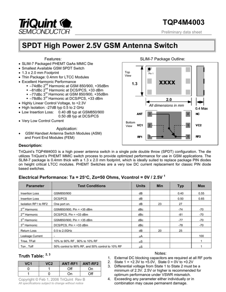
SPDT High Power 2.5V GSM Antenna Switch
Features:
•
•
•
•
•
•
•
•
•
SLIM-7 Package Outline:
SLIM-7 Packaged PHEMT GaAs MMIC Die
Smallest Available GSM SPDT Switch
1.3 x 2.0 mm Footprint
Thin Package: 0.4mm for LTCC Modules
Excellent Harmonic Performance
–74dBc 2nd Harmonic at GSM 850/900, +35dBm
–81dBc 2nd Harmonic at DCS/PCS, +33 dBm
–77dBc 3rd Harmonic at GSM 850/900, +35dBm
–78dBc 3rd Harmonic at DCS/PCS, +33 dBm
Highly Linear Control Voltage, to +2.3V
High Isolation: -27dB typ 0.5 to 2 GHz
Low Insertion Loss: 0.40 dB typ at GSM850/900
0.50 dB typ at DCS/PCS
Very Low Control Current
Application:
•
GSM Handset Antenna Switch Modules (ASM)
and Front End Modules (FEM)
Top
View
Pin 1
xxxx
+0.1
.1 / - 0.0
0.05
5
1.3 +0
1.3
.05
2.0 +0.1
2.0/ - 00.05
All dimensions in mm
0.4 Max
ANT
3
4
NC
Bottom
VC1
View
2
5
VC2
RF1
1
6
RF2
Description:
TriQuint’s TQP4M4003 is a high power antenna switch in a single pole double throw (SPDT) configuration. The die
utilizes TriQuint’s PHEMT MMIC switch process to provide optimized performance for use in GSM applications. The
SLIM-7 package is 0.4mm thick with a 1.3 x 2.0 mm footprint, which is ideally suited to replace package PIN diodes
on height critical LTCC modules. PHEMT Switches are a very low DC current replacement for classic PIN diode
based switches.
Electrical Performance: Ta = 25°C, Zo=50 Ohms, Vcontrol = 0V / 2.5V 1
Parameter
Test Conditions
Units
Min
Typ
Max
Insertion Loss
GSM850/900
dB
0.40
0.55
Insertion Loss
DCS/PCS
dB
0.50
0.65
Isolation RF1 to RF2
One port on.
dB
nd
GSM850/900, Pin = +35 dBm
dBc
-74
-70
nd
DCS/PCS, Pin = +33 dBm
dBc
-81
-70
rd
GSM850/900, Pin = +35 dBm
dBc
-77
-70
rd
DCS/PCS, Pin = +33 dBm
dBc
-78
-70
2 Harmonic
2 Harmonic
3 Harmonic
3 Harmonic
23
Return Loss
0.5 to 2.0GHz
dB
Leakage Current
-
µA
100
Trise, TFall
10% to 90% RF , 90% to 10% RF
µS
1
Ton , Toff
50% control to 90% RF, and 50% control to 10% RF
µS
1
VC2
1
0
25
Notes:
Truth Table: 2, 3
VC1
0
1
20
27
ANT-RF1
Off
On
ANT-RF2
On
Off
Copyright © Feb 1, 2006 TriQuint Rev B
All specifications subject to change without notice
1. External DC blocking capacitors are required at all RF ports
2. State 1 = +2.3V to +5.0V, State 0 = 0V to +0.2V
3. Differential voltage from State 1 to State 2 must be a
minimum of 2.3V. 2.5V or higher is recommended for
optimum performance under VSWR mismatch.
4. Exceeding any parameter either individually or in
combination may cause permanent damage.
TQP4M4003 Preliminary Datasheet
SPDT High Power 2.5V GSM Antenna Switch
Absolute Maximum Ratings4:
Pin Descriptions:
Parameter
Absolute Maximum
Max Input Power
+37dBm
Control Voltage
+/-5V
Operating Temp
-40°C to +85°C
Storage Temp
-65°C to +150°C
Pad
Number
Pin Name
Description
1
RF1
RF Port 1
2
VC1
Control RF Port 1
3
ANT
ANTENNA Port
4
NC
No Connection
5
VC2
Control RF Port 2
6
RF2
RF Port 2
Typical Performance Curves:
Insertion Loss and Match
Isolation
SPDT in SLIM-7 Package
Isolation, One RF port On (Vctrl=2.5v)
10
5
0
-5
-10
-15
-20
-25
-30
-35
-40
0.0
-0.1
-0.2
-0.3
-0.4
-0.5
-0.6
-0.7
-0.8
-0.9
-1.0
0.0
0.5
1.0
1.5
2.0
0.0
-5.0
-10.0
-15.0
-20.0
-25.0
-30.0
-35.0
-40.0
-45.0
-50.0
Return Loss (dB)
Insertion Loss (dB)
SPDT in SLIM-7 Package
RF1/RF2 to ANTENNA (Vctrl=2.5v)
0.0
2.5
Harmonics GSM850
26 27 28 29 30 31 32 33 34 35 36
Input Power (dBm)
Copyright © Feb 1, 2006 TriQuint Rev B
All specifications subject to change without notice
2.0
2.5
SPDT in SLIM-7 Package
GSM900 (Vctrl=2.5v F=897.5MHz)
Harmonics (dBc)
Harmonics (dBc)
H3
1.5
Harmonics GSM900
SPDT in SLIM-7 Package
GSM850 (Vctrl=2.5v F=836.5MHz)
H2
1.0
Frequency (GHz)
Frequency (GHz)
-20
-30
-40
-50
-60
-70
-80
-90
-100
-110
-120
0.5
-20
-30
-40
-50
-60
-70
-80
-90
-100
-110
-120
H2
H3
26 27 28 29 30 31 32 33 34 35 36
Input Power (dBm)
TQP4M4003 Preliminary Datasheet
SPDT High Power 2.5V GSM Antenna Switch
Harmonics DCS
Harmonics PCS
SPDT in SLIM-7 Package
PCS (Vctrl=2.5v F=1880MHz)
-20
-30
-40
-50
-60
-70
-80
-90
-100
-110
-120
H2
H3
Harmonics (dBc)
Harmonics (dBc)
SPDT in SLIM-7 Package
DCS (Vctrl=2.5v F=1747.5MHz)
-20
-30
-40
-50
-60
-70
-80
-90
-100
-110
-120
24 25 26 27 28 29 30 31 32 33 34
H2
H3
24 25 26 27 28 29 30 31 32 33 34
Input Power (dBm)
Input Power (dBm)
SLIM-7 Package
Top View
Bottom View
Side View
NOTES
1.1 All dimensions are in Millimeter (mm)
1.2 Package surface is mirror finish.
1.3 Dimensions are exclusive of mold flash and gate burr.
1.4 Lead finish is gold.
Copyright © Feb 1, 2006 TriQuint Rev B
All specifications subject to change without notice
TQP4M4003 Preliminary Datasheet
SPDT High Power 2.5V GSM Antenna Switch
Application Board:
Package Configuration On Board:
Application Board Loss De-Embedding Curve: FR4
Board Loss (dB)
0
-0.1
-0.2
-0.3
-0.4
-0.5
-0.6
0
0.5
1
1.5
Frequency (GHz)
Copyright © Feb 1, 2006 TriQuint Rev B
All specifications subject to change without notice
2
2.5
TQP4M4003 Preliminary Datasheet
SPDT High Power 2.5V GSM Antenna Switch
Part Marking:
where XXXX = last four digits of batch
Part Orientation on Reel:
Ordering Information:
Type
TQP4M4003
Marking
Package
XXXX
SLIM-7
ESD: Electrostatic Discharge Sensitive Device: Observe Handling Precautions!
Additional Information
For latest specifications, additional product information, worldwide sales and distribution locations, and information
about TriQuint:
Web: www.triquint.com
Email: info_wireless@tqs.com
Tel: (503) 615-9000
Fax: (503) 615-8902
For technical questions and additional information on specific applications:
Email: info_wireless@tqs.com
The information provided herein is believed to be reliable; TriQuint assumes no liability for inaccuracies or omissions.
TriQuint assumes no responsibility for the use of this information, and all such information shall be entirely at the
user's own risk. Prices and specifications are subject to change without notice. No patent rights or licenses to any of
the circuits described herein are implied or granted to any third party.
TriQuint does not authorize or warrant any TriQuint product for use in life-support devices and/or systems.
Copyright © 2006 TriQuint Semiconductor, Inc. All rights reserved.
Revision B Feb 1, 2006
For additional information and latest specifications, see our website: www.triquint.com
6
