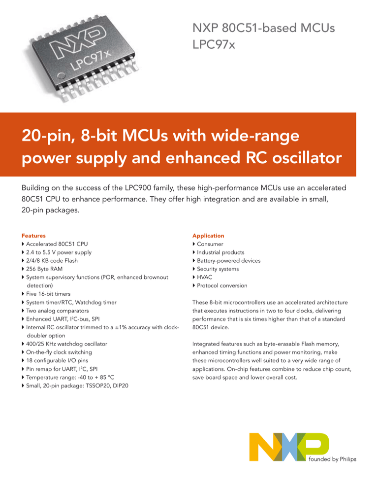
NXP 80C51-based MCUs
LPC97x
20-pin, 8-bit MCUs with wide-range
power supply and enhanced RC oscillator
Building on the success of the LPC900 family, these high-performance MCUs use an accelerated
80C51 CPU to enhance performance. They offer high integration and are available in small,
20-pin packages.
Features
} Accelerated 80C51 CPU
} 2.4 to 5.5 V power supply
} 2/4/8 KB code Flash
} 256 Byte RAM
}S
ystem supervisory functions (POR, enhanced brownout
detection)
} Five 16-bit timers
} System timer/RTC, Watchdog timer
} Two analog comparators
} Enhanced UART, I2C-bus, SPI
} Internal RC oscillator trimmed to a ±1% accuracy with clockdoubler option
} 400/25 KHz watchdog oscillator
} On-the-fly clock switching
} 18 configurable I/O pins
} Pin remap for UART, I2C, SPI
} Temperature range: -40 to + 85 °C
} Small, 20-pin package: TSSOP20, DIP20
Application
} Consumer
} Industrial products
} Battery-powered devices
} Security systems
} HVAC
} Protocol conversion
These 8-bit microcontrollers use an accelerated architecture
that executes instructions in two to four clocks, delivering
performance that is six times higher than that of a standard
80C51 device.
Integrated features such as byte-erasable Flash memory,
enhanced timing functions and power monitoring, make
these microcontrollers well suited to a very wide range of
applications. On-chip features combine to reduce chip count,
save board space and lower overall cost.
The LPC97x microcontroller has 2/4/8 KB of byte-erasable
Flash code memory that can be used to simulate an EEPROM,
with a full erase or program taking only 2 ms. It also has 256
bytes of Data RAM.
consumption in power-save modes. To reduce power
consumption further, each processor supports an idle mode
and two different power-down modes. Total power-down
current is less than 1 μA.
Serial interfaces include a 400 kHz I2C bus and an enhanced
UART with fractional baud-rate generator, break detect,
framing error detection, automatic address detection and
versatile interrupt capabilities. The Pin Remap feature allows
the UART/I2C interface to be remapped to other pins and
offers the possibility to add a SPI bus.
There are up to 18 I/O, each with a VDD operating range of
2.4 to 5.5 V.
There are five 16-bit counter/timers, each configurable to
toggle a port output on timer overflow or to act as a PWM
output.
Third-party development tools
Through third-party suppliers, NXP offers a range
of development and evaluation tools for its
microcontrollers. For the most current listing,
please visit www.nxp.com/microcontrollers.
LPC97x block diagram
A 7.37 MHz internal RC oscillator with a ±1% tolerance over
voltage and ambient temperature lets the microcontroller
operate without external oscillator components. Users can
adjust the internal RC oscillator to other frequencies. When
the clock doubler option is enabled, the output frequency is
14.746 MHz. The on-chip Watchdog timer has a separate
on-chip oscillator which provides two options: 400 kHz and
25 kHz, calibrated to ±10% at 400 kHz at room temperature.
It requires no external components, and is selectable from
eight values. To provide optimal support for active mode
with minimal power, there is on-the-fly clock switching for
the internal RC oscillator, the Watchdog oscillator, and the
external clock source. Fast switching maximizes performance.
System supervisory functions include Power-on reset (POR)
and enhanced brownout detection (BOD). Enhanced low-voltage
(brownout) detect allows a graceful system shutdown when
power fails and can be optionally configured as an interrupt.
The integrated real-time clock is equipped with independent
power and clock supplies, permitting extremely low power
Memory
2/4/8 kB Code Flash
256 byte Data RAM
Accelerated 2-Clock 80C51 CPU
System Supervisory Functions
(Power-on Reset, Robust Brownout Detect, clock switching on the fly)
System Timer/
Real-Time Clock
Timer 0/Timer 1
WDT w/OSC
Timer 2/Timer 3/Timer 4
Timers
Analog
Features
Analog Comparators
SPI[1]
Serial
Interfaces
I2C
UART
On-chip RC Oscillator
7.3728 MHz (w/clock doubler)
Keypad Interrupt
18 Configurable I/O Pins
002aae901
LPC970/971/972 selection guide
Type
Memory
Timers
2/3/4
I/O pins
256 B
•
4K
256 B
8K
256 B
Flash
RAM
P89LPC970
2K
P89LPC971
P89LPC972
[1]
ADC
Serial interfaces
Temperature
range (°C)
Package
I2C-bus
UART
SPI
18
•
•
• [1]
-40 to +85
TSSOP20
•
18
•
•
• [1]
-40 to +85
TSSOP20
•
18
•
•
•
-40 to +85
TSSOP20, DIP20
[1]
SPI available for pin remap
www.nxp.com
© 2009 NXP B.V.
All rights reserved. Reproduction in whole or in part is prohibited without the prior written consent of the copyright owner.
Date of release: September 2009
The information presented in this document does not form part of any quotation or contract, is believed to be accurate and
Document order number: 9397 750 16820
reliable and may be changed without notice. No liability will be accepted by the publisher for any consequence of its use.
Printed in the Netherlands
Publication thereof does not convey nor imply any license under patent- or other industrial or intellectual property rights.


