AN–PM–1007
SC632 5V-to-5V Regulation
Application Note
POWER MANAGEMENT
The SC632 is a high-current voltage regulator that uses
Semtech’s proprietary low-noise charge pump technology
to maintain a constant 5V output with input voltages
ranging from 2.9V to 5.5V. When the input is greater than
5.0V, the device provides the performance of a linear LDO
(Low Drop-Out) regulator. For input voltages below 5.0V,
the charge pump is activated. The charge pump control
system determines whether the device needs to boost the
input by 1.5x or 2x to maintain the output at 5.0V based
on the input voltage and load current conditions.
5V Input to 5V Output
The inherent function of the SC632 - to provide a 5V
output for any input voltage - makes this device especially
effective for applications requiring a stable 5V supply.
One such application involves taking a loosely-regulated
5V power rail and using it to produce a 5V supply with
improved regulation capability. A USB VBUS supply is a
good example of such a power rail. The USB specification
requires the voltage to be regulated within ±10% of the
nominal value. This means that the 5V supply could droop
5V VBUS
from USB
connector
CIN
22μF
as low as 4.5V, making it inadequate for systems that
require a well-regulated 5V supply.
Some users faced with this issue will simply regulate the
VBUS supply using an LDO regulator as a buffer to produce
a stable output. There are some drawback to this
approach. In general, the designer must set the output
voltage to a level less than the desired 5V to account for
the dropout of the LDO. Even when the VBUS supply is
higher than 5V, the designer must account for the case
when the supply is at 5V or below. A robust design using
an LDO would need to set the LDO output voltage less
than 4.5V - the minimum supply voltage available.
Operating the load at less than 5V is not always an acceptable option.
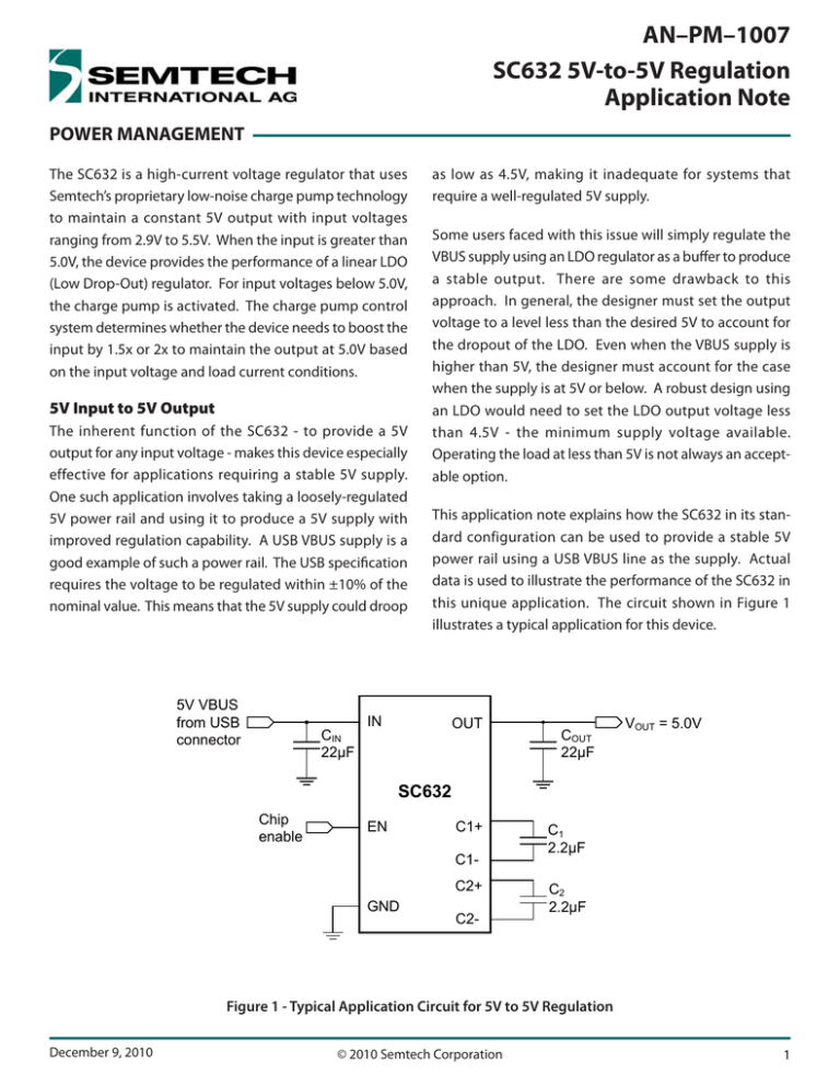
This application note explains how the SC632 in its standard configuration can be used to provide a stable 5V
power rail using a USB VBUS line as the supply. Actual
data is used to illustrate the performance of the SC632 in
this unique application. The circuit shown in Figure 1
illustrates a typical application for this device.
IN
OUT
COUT
22μF
VOUT = 5.0V
SC632
Chip
enable
EN
C1+
C1C2+
GND
C2-
C1
2.2μF
C2
2.2μF
Figure 1 - Typical Application Circuit for 5V to 5V Regulation
December 9, 2010
© 2010 Semtech Corporation
1
AN–PM–1007
Line Transient Response
The first parameter of interest for the 5V-to-5V regulation
application is line transient response. This term refers to
the output behavior of the SC632 in the presence of a line
voltage transient. One example of such a transient is the
scenario in which the input supply is a USB hub with
several slave devices connected to it. There is a limited
amount of supply current available in a hub device, so if
there is a large current demand on one slave device the
voltage level supplied to all slave devices could decrease
rapidly.
longer needed, the charge pump is automatically disabled
and 1x mode is restored.
Figure 3 illustrates SC632 performance when the input
supply varies between a noisy 5V level and a fixed 4.5V, as
shown by the bottom waveform (purple). The reference
point for both waveforms is set to 5V.
The waveforms in Figure 2 illustrate the response of the
SC632 when the input voltage drops from 5.5V to 4.5V.
The reference point for both waveforms is set to 5V.
Figure 3 - Line Transient Steady State Response
(100mA load)
Figure 2 - Line Transient Response (100mA load)
The bottom waveform (purple) shows the input supply
voltage stepping from 5.5V to 4.5V for a duration of 1.2ms
and then back to 5.5V. The SC632 starts in 1x (LDO) mode
in this scenario because the input supply is larger than
required to supply 100mA at the 5V output voltage level.
The top waveform (blue) shows how the output is maintained at approximately 5V until the input voltage drops.
During the fall time, the output voltage tracks the input
until the charge pump is activated. This process takes
approximately 40μs before the charge pump engages and
the output is boosted back to 5V. Once the output voltage
is returned to a level at which the charge pump is no
In this case, the top waveform (blue) shows the SC632 has
activated the charge pump in 1.5x mode to maintain the
output at 4.96V under load. Note that, aside from some
minor effects of switching transients, the output voltage
is regulated to 5V regardless of the input supply level. The
transients on the output waveform are between 50mV
and 100mV, or 1-2%, which is well within the voltage regulation requirements. Figure 3 also illustrates that the
SC632 rejects the noise on the 5V supply to provide a
cleaner 5V output, which is important for noise-sensitive
circuits such as those found in modems and other communications equipment.
In the steady state response, regulation is maintained to
within the ±3% range specified in the datasheet - even
during the transient events. If a linear LDO regulator had
been used, the device would have experienced drop out
while the supply was at 4.5V, which means the output
would have been unregulated and equal to the input
© 2010 Semtech Corporation
2
AN–PM–1007
Load Transient Response
Like line transients, load transients can adversely affect
regulation by putting a sudden current load demand on
the regulator. In systems using the VBUS 5V supply from a
USB master, it is not uncommon for the slave device to
have a large step in load current that can cause the 5V
supply to droop. In such situations, it is important to
recover quickly from this event and maintain proper regulation even while the supply voltage has sagged below
the expected 5V level.
The waveforms in Figure 4 show how the SC632 performs
under these conditions with its input supply fixed at 5.0V.
The stepped waveform (green) shows the load current
being switched from 10mA to 180mA. The top waveform
(blue) monitors the C2- pin voltage to show when the
charge pump is activated. The charge pump is active
when a switching waveform appears. The bottom waveform (purple) illustrates the output voltage response
during this stepped load event. The output sags to
approximately 4.93V for 140μs until the charge pump is
engaged and regulation is restored. The entire event takes
less than 200μs to restore regulation to expected levels.
Line and Load Regulation
Another possible application scenario involves an input
that varies widely over a specified range. For example, in
the case of a USB slave device that requires a regulated 5V,
it cannot expect that all masters have the same regulation
requirements designed into their power supply. In some
cases, the VBUS supply can be a tightly regulated 5V, but
in others it can be a poorly regulated supply that experiences drops in voltage as the load current demand
changes. Two parameters that describe the SC632’s ability
to adapt to this behavior are line regulation and load
regulation.
Line Regulation Performance
When a varying input supply is used, the SC632 can
provide a buffer by filtering out changes in line voltage. In
the plot shown in Figure 5, the input supply voltage is
varied from 4.5V to 5.5V and then back to 4.5V. Note that
the device switches modes during these transitions
without affecting the value of the output voltage.
5.1
ILOAD = 0mA
5.0
ILOAD = 200mA
4.9
Output Voltage (V)
supply voltage minus the I-R drop of the device. The
SC632 maintains regulation during the low-voltage duration so that the load can perform without loss of data.
4.8
4.7
4.6
LDO output
ILOAD = 200mA
4.5
4.4
4.5
4.7
4.9
5.1
5.3
5.5
Input Voltage (V)
Figure 5 - Line Regulation Performance
Figure 4 - Load Step Response
The data in Figure 5 illustrates how effective the SC632 is
at maintaining the output voltage even as the input
supply varies. The output voltage never drops below
4.97V. Note that the curve for the 200mA load condition
also shows regulation during LDO mode and charge pump
mode with hysteresis clearly displayed. This hysteresis is
used to keep the charge pump active as long as necessary
to ensure regulation is maintained and avoid mode tog© 2010 Semtech Corporation
3
AN–PM–1007
gling that can cause unwanted transient noise. By comparison, an LDO would not be able to provide the same
level of line regulation when the input voltage dropped
below 5.1V. The sloping waveform (green) shows data
collected using an LDO as the supply in the same
scenario.
Load Regulation Performance
Another parameter that illustrates the SC632 regulation
capability is load regulation. This parameter quantifies
the amount of output voltage variation as the load current
increases. Figure 6 illustrates the load regulation performance of the SC632 with the load current increased from
0mA to 200mA and the input supply set to 3 different settings: 4.5V, 5V, and 5.5V.
5.01
Output Voltage (V)
5
Other Considerations
The SC632’s simplicity is what makes it an ideal device to
provide 5V buffering capability. Figure 1 illustrates how a
circuit using the SC632 device and four external capacitors
satisfies this application. It is important to use the capacitance values recommended in the datasheet to ensure
proper regulation. When PCB area is not a concern, the
largest practical capacitance size should be used to ensure
the actual capacitance matches the nominal capacitor
values.
Proper low-noise layout techniques should always be followed as well. The SC632 datasheet provides a detailed
list of layout guidelines that will help ensure that device
performance is optimized. Compromising on these layout
guidelines could result in reduced performance of the
circuit and increased susceptibility to surrounding noise.
VIN = 5.5V
4.99
VIN = 5.0V
4.98
VIN = 4.5V
4.97
4.96
0
40
80
120
160
200
Load Current (mA)
Figure 6 - Load Regulation Performance
As with line regulation, the SC632 maintains the output
voltage above 4.97V even when the load is 200mA and
the input voltage is 4.5V. This capability is especially critical when the output voltage is supplying equipment that
requires a 5V power supply to ensure proper data transfer
or processing.
© 2010 Semtech Corporation
4
AN–PM–1007
© Semtech 2010
All rights reserved. Reproduction in whole or in part is prohibited without the prior written consent of the copyright
owner. The information presented in this document does not form part of any quotation or contract, is believed to be
accurate and reliable and may be changed without notice. No liability will be accepted by the publisher for any consequence of its use. Publication thereof does not convey nor imply any license under patent or other industrial or intellectual property rights. Semtech assumes no responsibility or liability whatsoever for any failure or unexpected operation
resulting from misuse, neglect improper installation, repair or improper handling or unusual physical or electrical stress
including, but not limited to, exposure to parameters beyond the specified maximum ratings or operation outside the
specified range.
SEMTECH PRODUCTS ARE NOT DESIGNED, INTENDED, AUTHORIZED OR WARRANTED TO BE SUITABLE FOR USE IN LIFESUPPORT APPLICATIONS, DEVICES OR SYSTEMS OR OTHER CRITICAL APPLICATIONS. INCLUSION OF SEMTECH PRODUCTS
IN SUCH APPLICATIONS IS UNDERSTOOD TO BE UNDERTAKEN SOLELY AT THE CUSTOMER’S OWN RISK. Should a customer
purchase or use Semtech products for any such unauthorized application, the customer shall indemnify and hold
Semtech and its officers, employees, subsidiaries, affiliates, and distributors harmless against all claims, costs damages
and attorney fees which could arise.
Contact Information
Taiwan
Tel: 886-2-2748-3380
Fax: 886-2-2748-3390
Switzerland
Tel: 41-32-729-4000
Fax: 41-32-729-4001
Korea
Tel: 82-2-527-4377
Fax: 82-2-527-4376
United Kingdom
Tel: 44-1794-527-600
Fax: 44-1794-527-601
Shanghai
Tel: 86-21-6391-0830
Fax: 86-21-6391-0831
France
Tel: 33-(0)169-28-22-00
Fax: 33-(0)169-28-12-98
Japan
Tel: 81-3-6408-0950
Fax: 81-3-6408-0951
Germany
Tel: 49-(0)8161-140-123
Fax: 49-(0)8161-140-124
www.semtech.com
© 2010 Semtech Corporation
5


