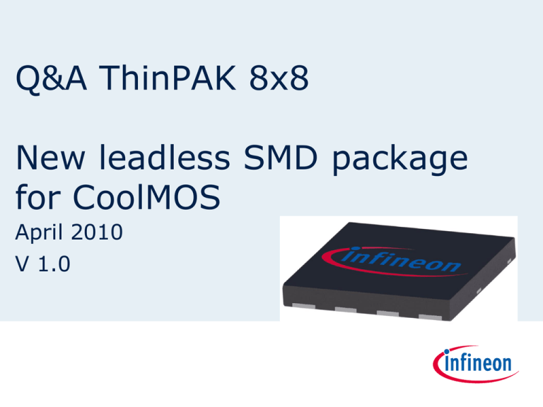
Q&A ThinPAK 8x8
New leadless SMD package
for CoolMOS
April 2010
V 1.0
Contents
Package outline
Manufacturing
Package quality
Materials and packing
Electrical and thermal characteristics
General
10.02.2010
2010-01-14
Copyright © Infineon Technologies 2010. All rights reserved.
Page 2
Contents
Package outline
Manufacturing
Package quality
Materials and packing
Electrical and thermal characteristics
General
10.02.2010
2010-01-14
Copyright © Infineon Technologies 2010. All rights reserved.
Page 3
3D view and pinning
1
8
8
leadless SMD package with
an exposed drain pad for
optimum heat transfer to
the PCB
Drain
Power Source
Pins
10.02.2010
Driver
Source
Pin
Copyright © Infineon Technologies 2010. All rights reserved.
Gate
Pin
Page 4
ThinPAK vs. D2PAK
10 x 15 x 4.4 mm³
8 x 8 x 1 mm³
60 % footprint reduction - 80% height reduction
10.02.2010
Copyright © Infineon Technologies 2010. All rights reserved.
Page 5
ThinPAK 8x8 – Package outline, Lead finishing
Lead finishing: pure tin plating
10.02.2010
Copyright © Infineon Technologies 2010. All rights reserved.
Page 6
Creepage distance
The creepage distance corresponds to the IPC9592 standard for
linear functional spacing requirements for an operational voltage
of 400 V
Creepage distance: 2.75 mm
10.02.2010
Copyright © Infineon Technologies 2010. All rights reserved.
Page 7
Contents
Package outline
Manufacturing
Package quality
Materials and packing
Electrical and thermal characteristics
General
10.02.2010
2010-01-14
Copyright © Infineon Technologies 2010. All rights reserved.
Page 8
Wave and reflow soldering
Is the package suited for wave soldering ?
Yes
What is the recommended reflow soldering temperature profile ?
Typically, the reflow profile depends on different factors like
solder paste, component mix, etc. One of these factors is the
package, which is qualified according J-STD-020D with a
maximum soldering temperature of 260°C. Details can be
found in the application note "Recommendations for board
assembly of ThinPAK 8x8"
10.02.2010
Copyright © Infineon Technologies 2010. All rights reserved.
Page 9
Board pad design
What is the recommended board pad design ?
10.02.2010
Copyright © Infineon Technologies 2010. All rights reserved.
Page 10
Stencil design
What is the recommended stencil design (apertures, stencil
thickness) ?
Typical stencil thickness 100 -150 µm
Stencil apertures
10.02.2010
Copyright © Infineon Technologies 2010. All rights reserved.
Page 11
Solder paste
What is the recommended solder paste (e.g. no clean solder
paste) ?
Lead containing (typically Sn63Pb37 or Sn62Pb36Ag2) as well
as lead free solder paste (typically Sn96.5Ag3Cu0.5) can be
used. A “no-clean” solder paste is preferred since cleaning
below the package is difficult. The paste must be suitable for
printing the solder stencil aperture dimensions; type 3 paste is
typical.
What are recommended Pick and Place process parameters ?
Minimum placement accuracy +/-150 µm;
Maximum force 10
N., Recognition is comparable to other tin plated leadless
packages
10.02.2010
Copyright © Infineon Technologies 2010. All rights reserved.
Page 12
Inspection, cleaning and rework
How can the solder joint quality be inspected ?
The solder joint meniscus of the 4 source/gate leads can be
inspected by optical microscope or AOI. If it is intended to
inspect the drain pad solder joint this can be done by X-ray
What are recommendations for cleaning the board ?
Since cleaning under the component is difficult we recommend
to use "no-clean" solder paste.Details can be found in the
application note "Recommendations for board assembly of
ThinPAK 8x8“
What is the reworking procedure for this package ?
It is recommended to use a rework station for rework to obtain
best quality and reliability. Using a soldering iron is not
recommended, using hot air gun may be possible but the
rework process can't be controlled accurately (e.g.
overheating).
10.02.2010
Copyright © Infineon Technologies 2010. All rights reserved.
Page 13
Contents
Package outline
Manufacturing
Package quality
Materials and packing
Electrical and thermal characteristics
General
10.02.2010
2010-01-14
Copyright © Infineon Technologies 2010. All rights reserved.
Page 14
Qualification
For which applications is this package qualified ?
The package is qualified for Server applications. Qualification
extension for industrial application is started
Is the package automotive qualified ?
No, the package is not qualified for automotive applications
What is the TCoB stability of this package ?
Internal TCoB -40/125°C on a 4 layer, 1.6 mm PCB show a
reliability of minimum 2000 cy.
What is the min/maximum operating temperature ?
Minmum operating temperature is -40°C, maximum operating
temperature is 150°C
10.02.2010
Copyright © Infineon Technologies 2010. All rights reserved.
Page 15
Qualification
What qualifications tests were performed ?
Pre-Conditioning prior to all tests (MSL3, 260°C)
Temperature cycling TC (-40/125°C), 500 cy.
Autoclave AC (121°C / 100% rh), 96 h.
High Humidity High Temp. Reverse Bias H3TRB (85°C / 85%rh V =
80V), 500 h.
High Temperature Reverse Bias HTRB (Ta =150°C,V = 540V), 500 h
High Temperature Gate stress HTGS (Ta =150°C, Vg = ±20V), 500 h
Intermittend Operational Life Test IOL (Delta T=100K ), 7500 cy.
10.02.2010
Copyright © Infineon Technologies 2010. All rights reserved.
Page 16
Contents
Package outline
Manufacturing
Package quality
Materials and packing
Electrical and thermal characteristics
General
10.02.2010
2010-01-14
Copyright © Infineon Technologies 2010. All rights reserved.
Page 17
Materials and packing
Is the package RoHS compliant ?
Yes, the package is RoHS compliant
Is the mold compound halogen free ?
Yes the package is halogen-free according to IEC61249-2-21
What is the MSL level of the package ?
The package is qualified for MSL 3, 260°C
What is the packing of the package ?
The package is packed in tape and reel (4" reel, pcs., 3.5
k/reel)
10.02.2010
Copyright © Infineon Technologies 2010. All rights reserved.
Page 18
Contents
Package outline
Manufacturing
Package quality
Materials and packing
Electrical and thermal characteristics
General
10.02.2010
2010-01-14
Copyright © Infineon Technologies 2010. All rights reserved.
Page 19
Advantages, Parasitic inductivity
What is the advantage of using this package in the application ?
The package gives different advantages:
¬ high power density,
¬ short commutation loop,
¬ very small drain source overshoots
¬ best behaviour for fast switching technologies
What is the parasitic inductivity of this package compared to
other packages like D2PAK and TO220 ?
The parasitic inductivity of the ThinPAK is 2 nH, D2PAK 6 nH
and for TO220 depending on the leadlength between 6 and 12
nH
What is the advantage of using a low parasitic package ?
A low inductive package minimizes overshoots and is easy to
use
10.02.2010
Copyright © Infineon Technologies 2010. All rights reserved.
Page 20
Power capability
What power can the package handle ?
This depends on the product used and on the thermal system.
In an optimized cooling system a thermal resistance of 10 K/W
is feasible when using a heatsink and forced convection. This
would mean a power of 5 to 7 W is feasible.
What is the maximum current, pulse current ?
Max. current: this depends on the product. For the
IPL60R199CP continous current: 16 A pulse current 51 A (Tc =
25°C)
How does the efficiency compare to other package types ?
There is no significant difference in terms of efficiency
compared to traditional SMD packages
10.02.2010
Copyright © Infineon Technologies 2010. All rights reserved.
Page 21
Waveform, thermal performance
What does the waveform look like compared to packages like
D2PAK and TO220 ?
The low parasitic inductivity results in a very smooth
waveform with minumim ringing and overshoots.
How is the thermal performance in comparsion to a D2PAK ?
The thermal performance is similar to existing traditional SMD
packages like the D2PAK
What is an optimized thermal sytem (Heatsink, interface
material, board design) ?
The ThinPAK features an exposed drainpad. Therefore the
dominant heatpath is to the PCB. To increase the power
capability the usage of a heatsink which is mounted on the
bottom side of the PCB is recommended. To keep the thermal
resistance through the PCB low the PCB shall be designed with
many vias (e.g. 40 or even more)
10.02.2010
Copyright © Infineon Technologies 2010. All rights reserved.
Page 22
Layout, thermal resistances
What is a optimized layout ?
Please see the application note: CoolMOSTM CP - How to make
most beneficial use of the latest generation of super junction
technology devices
What is the optimized layout for paralleling ?
The use of a common source layer is recommended
What is the thermal resistance Rthjc, Rthja ?
For IPL60R199CP the Rthjc is max. 0.9 K/W
The Rthja for 600 mm², 70 µm Cu, single layer board is max.
42 K/W
Can this package be used for top-side cooling ?
Yes, but one has to consider that the thermal resistance to the
top side is higher than to the bottom side which results in a
dominant heatflow to the PCB
10.02.2010
Copyright © Infineon Technologies 2010. All rights reserved.
Page 23
Rthjc_top, Spice Models, Gate resistor
What is the Rthjc to the top side ?
For IPL60R199CP the Rthjc to the top side is ~ 30 K/W
Are spice models available ?
Yes, they can be downloaded from the Infineon homepage
What is the optimum gate resistor ?
Please see the application note: CoolMOSTM CP - How to make
most beneficial use of the latest generation of super junction
technology devices
10.02.2010
Copyright © Infineon Technologies 2010. All rights reserved.
Page 24
Contents
Package outline
Manufacturing
Package quality
Materials and packing
Electrical and thermal characteristics
General
10.02.2010
2010-01-14
Copyright © Infineon Technologies 2010. All rights reserved.
Page 25
Applications and products
What are typical applications ?
Applications are high power density designs from server to
adapter
Which products are available ?
10.02.2010
Copyright © Infineon Technologies 2010. All rights reserved.
Page 26
Product outlook and 2nd source
Are there plans for other products
There are plans to increase the portfolio and to have the SiC
diodes in this package
Is there a 2nd source available ?
ST Microelectronics has the same package which has the same
outline.
What are the difference between ST and IFX package ?
Both packages are the same from an outline perspective. The
same board pad design can be used
Do ST and IFX manufacture in the same location ?
No, both campanies produce at different locations
10.02.2010
Copyright © Infineon Technologies 2010. All rights reserved.
Page 27
