AN-751
APPLICATION NOTE
One Technology Way • P.O. Box 9106 • Norwood, MA 02062-9106, U.S.A. • Tel: 781.329.4700 • Fax: 781.461.3113 • www.analog.com
High Speed Universal Op Amp Evaluation Board with Exposed Paddle
by John Ardizzoni
The assembly drawings are shown in Figure 3 through Figure 6.
The Analog Devices, Inc., high speed, universal evaluation
boards are designed to help customers quickly prototype and
evaluate new designs. This application note covers two evaluation boards, the EVAL-ADOPAMP-1REZ (for 8-lead SOICs)
and the EVAL-ADOPAMP-1CPEZ (for 8-lead LFCSPs). These
evaluation boards are designed for amplifiers that require a
voltage potential on the exposed paddle, such as the AD8045.
However, these boards can also be used with standard SOIC
and LFCSP packages. These evaluation boards, unlike other
evaluation boards, have both an inverting and noninverting
amplifier circuit on the same board. The two amplifier circuits
are completely independent.
The ground plane, component placement, and supply bypassing are laid out to minimize parasitic elements and provide
optimum high frequency performance. The board SMT
components are primarily 0603 case size, with the exception of
the electrolytic bypass capacitors, C1 and C4. If designers want
to incorporate any of the aspects of the evaluation board layout
into their design, the board layout patterns are included as
shown in Figure 7 through Figure 10.
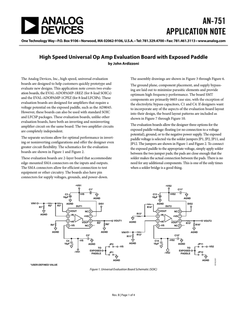
The evaluation boards allow the designer three options for the
exposed paddle voltage: floating (or no connection to a voltage
potential), ground, or to the negative power supply. The exposed
paddle voltage is selected via the solder jumpers JP1, JP2, JP11, and
JP12. The jumpers are shown in Figure 1 and Figure 2. To connect
the exposed paddle to the appropriate voltage, simply apply solder
between the two jumper pads; the pads are close enough that the
solder makes the actual connection between the pads. There is no
need for any additional components. This is one of the only times
when a solder bridge is a good thing.
The separate sections allow for optimal performance in inverting or noninverting configurations and offer the designer even
greater circuit flexibility. The schematics for the evaluation
boards are shown in Figure 1 and Figure 2.
These evaluation boards are 2-layer board that accommodate
edge-mounted SMA connectors on the inputs and outputs.
The SMA connectors allow for efficient connection to test
equipment or other circuitry. The boards also have pin
connectors for supply voltages, grounds, and power-down.
+VS1
+VS2
C11*
C1*
+VS
VIN1
R1*
R2*
R3*
AGND
DIS1
AGND
2
1 VOUT
R13*
+VS 7
3 +IN
R4*
2
VOUT1
6
VOUT
NC 5
4 –VS
AGND
R5*
R15*
AGND
JP2
VOUT2
R16*
AGND
–VS
–VS1
6
VOUT
NC 5
VIN1
R11*
TO
EXPOSED
PADDLE
+VS 7
4 –VS
AGND
AGND
NC 8
–IN
3 +IN
AGND
R6*
C2*
C4
10µF +
DIS2
DUT2
R14*
NC 8
–IN
AGND
AGND
DUT1
1 VOUT
AGND
+VS2
C13 +
10µF
R12*
C12*
C14
10µF
–VS2
AGND
+
–VS
JP1
AGND
*USER-DEFINED VALUE
Figure 1. Universal Evaluation Board Schematic (SOIC)
Rev. B | Page 1 of 4
–VS2
TO
EXPOSED
PADDLE
JP11
–VS2
JP12
AGND
05142-001
C3 +
10µF
AN-751
Application Note
+VS1
+VS2
C1*
C1*
DIS2
+VS
C3 +
10µF
AGND
AGND
R2*
R1*
R3*
1 NC
DUT2
+VS 8
2 VFB
3 –IN
NC 6
4 +IN
–VS 5
AGND
C2*
AGND
JP1
–VS1
TO
EXPOSED
PADDLE
3 –IN
NC 6
VOUT2
4 +IN
–VS 5
R16*
AGND
C12*
VIN1
–VS
+
VOUT 7
R15*
R13*
R6*
AGND
+VS 8
2 VFB
VOUT1
R4*
C4
10µF
1 NC
R14*
VOUT 7
R5*
AGND
AGND
AGND
DUT1
VIN1
+VS
C13 +
10µF
R11*
R12*
JP11
AGND
AGND
JP2
–VS1
TO
EXPOSED
PADDLE
–VS2
C14
10µF
–VS
AGND
+
JP12
–VS2
AGND
AGND
05142-002
DIS1
*USER-DEFINED VALUE
Figure 2. Universal Evaluation Board Schematic (LFCSP)
R1
R4
R3
EVAL-ADOPAMP-1R-EZ
+VS1
GND1 DUT1
C3
DIS1
JP1
VIN1
C1
R2
R5
VOUT1
R6
C2 GND3
JP2
VOUT1
C4
INVERTING
–VS1
+VS2
R14
R13
C13
DIS2
C11
JP12
R15
VOUT2
R16
C12GND4
NON-INVERTING
VOUT2
A00973B
C14
–VS2
COMPONENT SIDE
CIRCUIT SIDE
05142-004
R12
JP11
05142-003
VIN2
R11
GND2 DUT2
Figure 5. Board Assembly Drawing (SOIC)
Figure 3. Board Assembly Drawing (SOIC)
JP2
EVAL-ADOPAMP-1CP-EZ
+VS1
GND1
R3
DIS1
VIN1
R4
JP1
R1
R2
C3
C1 DUT1
R5
VOUT1
R6
C2
C4
INVERTING
VOUT1
GND3
–VS1
R12
C13 DUT2
R15
R16 VOUT2
C14
NON-INVERTING
VOUT2
C12
A00975B
GND4
–VS2
COMPONENT SIDE
CIRCUIT SIDE
Figure 6. Board Assembly Drawing (LFSCP)
Figure 4. Board Assembly Drawing (LFCSP)
Rev. B | Page 2 of 4
05142-006
R13
JP12
VIN2
R11
DIS2
05142-005
R14
JP11
GND2 +VS2
COMPONENT SIDE
Figure 9. Board Layout Patterns (SOIC)
05142-009
Figure 7. Board Layout Patterns (SOIC)
05142-008
CIRCUIT SIDE
CIRCUIT SIDE
Figure 8. Board Layout Patterns (LFCSP)
Figure 10. Board Layout Patterns (LFCSP)
Rev. B | Page 3 of 4
05142-010
COMPONENT SIDE
AN-751
05142-007
Application Note
AN-751
Application Note
NOTES
©2004–2008 Analog Devices, Inc. All rights reserved. Trademarks and
registered trademarks are the property of their respective owners.
AN05142-0-9/08(B)
Rev. B | Page 4 of 4
