DRAM Circuit and Architecture Basics - ECE
advertisement

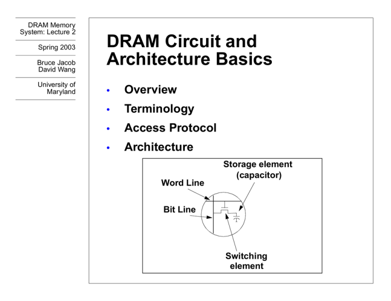
DRAM Memory System: Lecture 2 Spring 2003 Bruce Jacob David Wang University of Maryland DRAM Circuit and Architecture Basics • Overview • Terminology • Access Protocol • Architecture Word Line Storage element (capacitor) Bit Line Switching element DRAM Memory System: Lecture 2 Spring 2003 Bruce Jacob David Wang DRAM Circuit Basics DRAM Cell University of Maryland DRAM Word Line Storage element (capacitor) Column Decoder Sense Amps Data In/Out Buffers ... Bit Lines... . .. Word Lines ... Switching element Row Decoder Bit Line Memory Array DRAM Memory System: Lecture 2 Row, Bitlines and Wordlines Spring 2003 Bruce Jacob David Wang DRAM Circuit Basics “Row” Defined University of Maryland Bit Lines Word Line “Row” of DRAM Row Size: 8 Kb @ 256 Mb SDRAM node 4 Kb @ 256 Mb RDRAM node DRAM Memory System: Lecture 2 Spring 2003 Bruce Jacob David Wang DRAM Circuit Basics Sense Amplifier I University of Maryland 1 4 2 5 3 6 6 Rows shown Sense and Amplify DRAM Memory System: Lecture 2 Spring 2003 Bruce Jacob David Wang University of Maryland DRAM Circuit Basics Sense Amplifier II : Precharged precharged to Vcc/2 1 Vcc (logic 1) 4 Sense and Amplify 2 5 3 6 Gnd (logic 0) Vcc/2 DRAM Memory System: Lecture 2 Spring 2003 Bruce Jacob David Wang DRAM Circuit Basics Sense Amplifier III : Destructive Read University of Maryland 1 4 2 3 Vcc (logic 1) Gnd (logic 0) 5 Sense and Amplify 6 Wordline Driven Vcc/2 DRAM Memory System: Lecture 2 Spring 2003 Bruce Jacob David Wang DRAM Access Protocol ROW ACCESS University of Maryland DRAM Column Decoder Sense Amps Data In/Out Buffers . .. Word Lines ... AKA: OPEN a DRAM Page/Row or ACT (Activate a DRAM Page/Row) or RAS (Row Address Strobe) ... Bit Lines... Row Decoder CPU MEMORY BUS CONTROLLER Memory Array DRAM Memory System: Lecture 2 Spring 2003 Bruce Jacob David Wang University of Maryland once the data is valid on ALL of the bit lines, you can select a subset of the bits and send them to the output buffers ... CAS picks one of the bits big point: cannot do another RAS or precharge of the lines until finished reading the column data ... can’t change the values on the bit lines or the output of the sense amps until it has been read by the memory controller DRAM Circuit Basics “Column” Defined Column: Smallest addressable quantity of DRAM on chip SDRAM*: column size == chip data bus width (4, 8,16, 32) RDRAM: column size != chip data bus width (128 bit fixed) SDRAM*: get “n” columns per access. n = (1, 2, 4, 8) RDRAM: get 1 column per access. 4 bit wide columns #0 #1 #2 #3 #4 #5 “One Row” of DRAM * SDRAM means SDRAM and variants. i.e. DDR SDRAM DRAM Memory System: Lecture 2 Spring 2003 Bruce Jacob David Wang DRAM Access Protocol COLUMN ACCESS I University of Maryland DRAM Column Decoder Sense Amps Data In/Out Buffers . .. Word Lines ... READ Command or CAS: Column Address Strobe ... Bit Lines... Row Decoder CPU MEMORY BUS CONTROLLER Memory Array DRAM Memory System: Lecture 2 Spring 2003 Bruce Jacob David Wang DRAM Access Protocol Column Access II University of Maryland DRAM then the data is valid on the data bus ... depending on what you are using for in/out buffers, you might be able to overlap a litttle or a lot of the data transfer with the next CAS to the same page (this is PAGE MODE) Column Decoder Sense Amps Data In/Out Buffers . .. Word Lines ... Data Out ... Bit Lines... Row Decoder CPU MEMORY BUS CONTROLLER Memory Array ... with optional additional CAS: Column Address Strobe note: page mode enables overlap with CAS DRAM Memory System: Lecture 2 Spring 2003 Bruce Jacob David Wang University of Maryland DRAM “Speed” Part I How fast can I move data from DRAM cell to sense amp? NOTE DRAM Column Decoder Sense Amps Data In/Out Buffers RCD (Row Command Delay) . .. Word Lines ... tRCD ... Bit Lines... Row Decoder CPU MEMORY BUS CONTROLLER Memory Array Bruce Jacob David Wang University of Maryland DRAM “Speed” Part II How fast can I get data out of sense amps back into memory controller? tCAS aka tCASL aka tCL DRAM Column Decoder Sense Amps Data In/Out Buffers CPU MEMORY BUS CONTROLLER CAS: Column Address Strobe CASL: Column Address Strobe Latency CL: Column Address Strobe Latency ... Bit Lines... . .. Word Lines ... Spring 2003 Row Decoder DRAM Memory System: Lecture 2 Memory Array Bruce Jacob David Wang University of Maryland DRAM “Speed” Part III How fast can I move data from DRAM cell into memory controller? DRAM Column Decoder Sense Amps Data In/Out Buffers CPU MEMORY BUS CONTROLLER tRAC = tRCD + tCAS RAC (Random Access Delay) ... Bit Lines... . .. Word Lines ... Spring 2003 Row Decoder DRAM Memory System: Lecture 2 Memory Array Bruce Jacob David Wang University of Maryland DRAM “Speed” Part IV How fast can I precharge DRAM array so I can engage another RAS? DRAM Column Decoder Sense Amps Data In/Out Buffers CPU MEMORY BUS CONTROLLER tRP RP (Row Precharge Delay) ... Bit Lines... . .. Word Lines ... Spring 2003 Row Decoder DRAM Memory System: Lecture 2 Memory Array DRAM Memory System: Lecture 2 Spring 2003 Bruce Jacob David Wang DRAM “Speed” Part V How fast can I read from different rows? University of Maryland DRAM Column Decoder Sense Amps Data In/Out Buffers tRC = tRAS + tRP RC (Row Cycle Time) . .. Word Lines ... ... Bit Lines... Row Decoder CPU MEMORY BUS CONTROLLER Memory Array DRAM Memory System: Lecture 2 Spring 2003 Bruce Jacob David Wang University of Maryland DRAM “Speed” Summary I What do I care about? tRCD tCAS Seen in ads. Easy to explain Easy to sell tRP tRC = tRAS + tRP tRAC = tRCD + tCAS Embedded systems designers DRAM manufactuers Computer Architect: Latency bound code i.e. linked list traversal RAS: Row Address Strobe CAS: Column Address Strobe RCD: Row Command Delay RAC :Random Access Delay RP :Row Precharge Delay RC :Row Cycle Time DRAM Memory System: Lecture 2 Spring 2003 DRAM “Speed” Summary II Bruce Jacob David Wang DRAM Type Frequency Data Bus Width (per chip) Peak Data Bandwidth (per Chip) Random Access Time (tRAC) Row Cycle Time (tRC) PC133 SDRAM 133 16 200 MB/s 45 ns 60 ns DDR 266 133 * 2 16 532 MB/s 45 ns 60 ns PC800 RDRAM 400 * 2 16 1.6 GB/s 60 ns 70 ns FCRAM 200 * 2 16 0.8 GB/s 25 ns 25 ns RLDRAM 300 * 2 32 2.4 GB/s 25 ns 25 ns University of Maryland DRAM is “slow” But doesn’t have to be tRC < 10ns achievable Higher die cost Not commodity Not adopted in standard Expensive DRAM Memory System: Lecture 2 Spring 2003 “DRAM latency” F Bruce Jacob David Wang University of Maryland DRAM “latency” isn’t deterministic because of CAS or RAS+CAS, and there may be significant queuing delays within the CPU and the memory controller Each transaction has some overhead. Some types of overhead cannot be pipelined. This means that in general, longer bursts are more efficient. DRAM CPU Mem E1 Controller A B C D E2/E3 A: Transaction request may be delayed in Queue B: Transaction request sent to Memory Controller C: Transaction converted to Command Sequences (may be queued) D: Command/s Sent to DRAM E1: Requires only a CAS or E2: Requires RAS + CAS or E3: Requires PRE + RAS + CAS F: Transaction sent back to CPU “DRAM Latency” = A + B + C + D + E + F DRAM Memory System: Lecture 2 Spring 2003 Bruce Jacob David Wang DRAM Architecture Basics PHYSICAL ORGANIZATION University of Maryland NOTE x2 DRAM Sense Amps Data Buffers ... Bit Lines... Memory Array x4 DRAM This is per bank … Typical DRAMs have 2+ banks Column Decoder Sense Amps Data Buffers ... Bit Lines... .... Memory Array x8 DRAM Column Decoder Row Decoder .... ... Bit Lines... x4 DRAM .... Sense Amps Data Buffers Row Decoder Column Decoder Row Decoder x2 DRAM Memory Array x8 DRAM DRAM Memory System: Lecture 2 Spring 2003 Bruce Jacob David Wang DRAM Architecture Basics Read Timing for Conventional DRAM University of Maryland let’s look at the interface another way .. the say the data sheets portray it. RAS Row Access [explain] main point: the RAS\ and CAS\ signals directly control the latches that hold the row and column addresses ... Column Access CAS Data Transfer Address Row Address DQ Column Address Row Address Valid Dataout Column Address Valid Dataout DRAM Memory System: Lecture 2 Spring 2003 DRAM Evolutionary Tree ........ Bruce Jacob David Wang ...... University of Maryland MOSYS since DRAM’s inception, there have been a stream of changes to the design, from FPM to EDO to Burst EDO to SDRAM. the changes are largely structural modifications -- nimor -- that target THROUGHPUT. [discuss FPM up to SDRAM Everything up to and including SDRAM has been relatively inexpensive, especially when considering the pay-off (FPM was essentially free, EDO cost a latch, PBEDO cost a counter, SDRAM cost a slight re-design). however, we’re run out of “free” ideas, and now all changes are considered expensive ... thus there is no consensus on new directions and myriad of choices has appeared [ do LATENCY mods starting with ESDRAM ... and then the INTERFACE mods ] FCRAM Conventional DRAM $ (Mostly) Structural Modifications Targeting Throughput FPM Structural Modifications Targeting Latency EDO P/BEDO VCDRAM SDRAM ESDRAM Interface Modifications Targeting Throughput Rambus, DDR/2 Future Trends DRAM Memory System: Lecture 2 Spring 2003 Bruce Jacob David Wang DRAM Evolution Read Timing for Conventional DRAM University of Maryland Row Access NOTE Column Access Transfer Overlap Data Transfer RAS CAS Address Row Address DQ Column Address Row Address Valid Dataout Column Address Valid Dataout DRAM Memory System: Lecture 2 Spring 2003 Bruce Jacob David Wang DRAM Evolution Read Timing for Fast Page Mode University of Maryland Row Access FPM aallows you to keep th esense amps actuve for multiple CAS commands ... Column Access Transfer Overlap much better throughput problem: cannot latch a new value in the column address buffer until the read-out of the data is complete Data Transfer RAS CAS Address Row Address DQ Column Address Column Address Valid Dataout Column Address Valid Dataout Valid Dataout DRAM Memory System: Lecture 2 Spring 2003 Bruce Jacob David Wang DRAM Evolution Read Timing for Extended Data Out University of Maryland Row Access solution to that problem -instead of simple tri-state buffers, use a latch as well. by putting a latch after the column mux, the next column address command can begin sooner Column Access Transfer Overlap Data Transfer RAS CAS Address Row Address DQ Column Address Column Address Valid Dataout Column Address Valid Dataout Valid Dataout DRAM Memory System: Lecture 2 Spring 2003 Bruce Jacob David Wang DRAM Evolution Read Timing for Burst EDO University of Maryland Row Access by driving the col-addr latch from an internal counter rather than an external signal, the minimum cycle time for driving the output bus was reduced by roughly 30% Column Access Transfer Overlap Data Transfer RAS CAS Address Row Address DQ Column Address Valid Data Valid Data Valid Data Valid Data DRAM Memory System: Lecture 2 Spring 2003 Bruce Jacob David Wang DRAM Evolution Read Timing for Pipeline Burst EDO University of Maryland “pipeline” refers to the setting up of the read pipeline ... first CAS\ toggle latches the column address, all following CAS\ toggles drive data out onto the bus. therefore data stops coming when the memory controller stops toggling CAS\ Row Access Column Access Transfer Overlap Data Transfer RAS CAS Address Row Address DQ Column Address Valid Data Valid Data Valid Data Valid Data DRAM Memory System: Lecture 2 Spring 2003 Bruce Jacob David Wang DRAM Evolution Read Timing for Synchronous DRAM University of Maryland main benefit: frees up the CPU or memory controller from having to control the DRAM’s internal latches directly ... the controller/CPU can go off and do other things during the idle cycles instead of “wait” ... even though the time-to-first-word latency actually gets worse, the scheme increases system throughput Row Access Clock Column Access RAS Transfer Overlap Data Transfer CAS Command ACT READ Address Row Addr DQ Col Addr Valid Data Valid Data Valid Data Valid Data (RAS + CAS + OE ... == Command Bus) DRAM Memory System: Lecture 2 Spring 2003 Bruce Jacob David Wang University of Maryland output latch on EDO allowed you to start CAS sooner for next accesss (to same row) latch whole row in ESDRAM -allows you to start precharge & RAS sooner for thee next page access -- HIDE THE PRECHARGE OVERHEAD. DRAM Evolution Inter-Row Read Timing for ESDRAM “Regular” CAS-2 SDRAM, R/R to same bank Clock Command ACT READ PRE ACT READ Col Addr Bank Row Addr Col Addr Address Row Addr DQ Valid Data Valid Data Valid Data Valid Data Valid Data ESDRAM, R/R to same bank Clock Command ACT READ PRE ACT READ Col Addr Bank Row Addr Col Addr Address Row Addr DQ Valid Data Valid Data Valid Data Valid Data Valid Data Valid Data Valid Data Valid Data Valid Data Valid Data Valid Data DRAM Memory System: Lecture 2 Spring 2003 Bruce Jacob David Wang University of Maryland neat feature of this type of buffering: write-around DRAM Evolution Write-Around in ESDRAM “Regular” CAS-2 SDRAM, R/W/R to same bank, rows 0/1/0 Clock Command ACT READ PRE ACT WRITE PRE ACT READ Col Addr Bank Row Addr Col Addr Bank Row Addr Col Addr Address Row Addr DQ Valid Data Valid Data Valid Data Valid Data Valid Data Valid Data Valid Data Valid Data Valid Data ESDRAM, R/W/R to same bank, rows 0/1/0 Clock Command ACT READ PRE ACT WRITE READ Col Addr Row Addr Col Addr Col Addr Valid Valid Data Data Valid Data Address Row Addr DQ Bank Valid Data Valid Data Valid Data Valid Valid Data Data Valid Valid Data Data Valid Valid Data Data (can second READ be this aggressive?) Valid Data Valid Data DRAM Memory System: Lecture 2 Spring 2003 DRAM Evolution $ Bruce Jacob David Wang University of Maryland main thing ... it is like having a bunch of open row buffers (a la rambus), but the problem is that you must deal with the cache directly (move into and out of it), not the DRAM banks ... adds an extra couple of cycles of latency ... however, you get good bandwidth if the data you want is cache, and you can “prefetch” into cache ahead of when you want it ... originally targetted at reducing latency, now that SDRAM is CAS-2 and RCD-2, this make sense only in a throughput way Internal Structure of Virtual Channel 16 “Channels” (segments) Bank B Bank A Input/Output Buffer 2Kb Segment 2Kb Segment 2Kbit # DQs DQs 2Kb Segment 2Kb Segment Row Decoder Activate Sense Amps Prefetch Restore Sel/Dec Read Write Segment cache is software-managed, reduces energy DRAM Memory System: Lecture 2 Spring 2003 Bruce Jacob David Wang DRAM Evolution Internal Structure of Fast Cycle RAM University of Maryland SDRAM FCRAM 13 bits 8M Array (8Kr x 1Kb) Sense Amps tRCD = 15ns (two clocks) 15 bits Row Decoder 8K rows requires 13 bits tto select ... FCRAM uses 15 (assuming the array is 8k x 1k ... the data sheet does not specify) Row Decoder FCRAM opts to break up the data array .. only activate a portion of the word line 8M Array (?) Sense Amps tRCD = 5ns (one clock) Reduces access time and energy/access Spring 2003 Bruce Jacob David Wang DRAM Evolution ........ DRAM Memory System: Lecture 2 ...... Internal Structure of MoSys 1T-SRAM University of Maryland MoSys takes this one step further ... DRAM with an SRAM interface & speed but DRAM energy [physical partitioning: 72 banks] addr Bank Select auto refresh -- how to do this transparently? the logic moves tthrough the arrays, refreshing them when not active. but what is one bank gets repeated access for a long duration? all other banks will be refreshed, but that one will not. solution: they have a bank-sized CACHE of lines ... in theory, should never have a problem (magic) Auto Refresh $ DQs

