1SMC 5.0 ~ 188A
advertisement
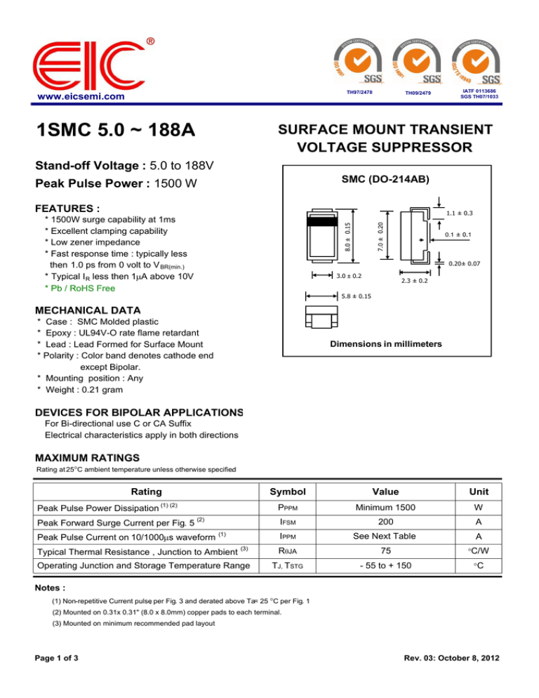
TH97/2478 www.eicsemi.com 1SMC 5.0 ~ 188A TH09/2479 IATF 0113686 SGS TH07/1033 SURFACE MOUNT TRANSIENT VOLTAGE SUPPRESSOR Stand-off Voltage : 5.0 to 188V SMC (DO-214AB) Peak Pulse Power : 1500 W FEATURES : 8.0 ± 0.15 7.0 ± 0.20 1.1 ± 0.3 * 1500W surge capability at 1ms * Excellent clamping capability * Low zener impedance * Fast response time : typically less then 1.0 ps from 0 volt to V BR(min.) * Typical I R less then 1μA above 10V * Pb / RoHS Free 0.1 ± 0.1 0.20± 0.07 3.0 ± 0.2 2.3 ± 0.2 5.8 ± 0.15 MECHANICAL DATA * Case : SMC Molded plastic * Epoxy : UL94V-O rate flame retardant * Lead : Lead Formed for Surface Mount * Polarity : Color band denotes cathode end except Bipolar. * Mounting position : Any * Weight : 0.21 gram Dimensions in millimeters DEVICES FOR BIPOLAR APPLICATIONS For Bi-directional use C or CA Suffix Electrical characteristics apply in both directions MAXIMUM RATINGS Rating at 25°C ambient temperature unless otherwise specified . Rating Peak Pulse Power Dissipation (1) (2) Peak Forward Surge Current per Fig. 5 (2) Peak Pulse Current on 10/1000μs waveform (1) Typical Thermal Resistance , Junction to Ambient (3) Operating Junction and Storage Temperature Range Symbol Value Unit PPPM Minimum 1500 W IFSM 200 A IPPM See Next Table A RθJA 75 °C/W TJ, TSTG - 55 to + 150 °C Notes : (1) Non-repetitive Current pulse, per Fig. 3 and derated above Ta= 25 °C per Fig. 1 (2) Mounted on 0.31x 0.31" (8.0 x 8.0mm) copper pads to each terminal. (3) Mounted on minimum recommended pad layout Page 1 of 3 Rev. 03: October 8, 2012 TH97/2478 www.eicsemi.com TH09/2479 ELECTRICAL CHARACTERISTICS (Rating at 25°C ambient temperature unless otherwise specified) Breakdown Voltage @ IT (1) Type No. VBR (V) Min. Max. IT (mA) Working Peak Reverse Voltage VWM (V) Maximum Reverse Leakage @ VWM ID (μA) 1SMC5.0A 6.40 7.07 10 5.0 1000 1SMC6.0A 6.67 7.37 10 6.0 1000 1SMC6.5A 7.22 7.98 10 6.5 500 1SMC7.0A 7.78 8.6 10 7.0 200 1SMC7.5A 8.33 9.21 1.0 7.5 100 1SMC8.0A 8.89 9.83 1.0 8.0 50 1SMC8.5A 9.44 10.4 1.0 8.5 20 1SMC9.0A 10.0 11.1 1.0 9.0 10 1SMC10A 11.1 12.3 1.0 10 5.0 1SMC11A 12.2 13.5 1.0 11 5.0 1SMC12A 13.3 14.7 1.0 12 5.0 1SMC13A 14.4 15.9 1.0 13 5.0 1SMC14A 15.6 17.2 1.0 14 5.0 1SMC15A 16.7 18.5 1.0 15 5.0 1SMC16A 17.8 19.7 1.0 16 5.0 1SMC17A 18.9 20.9 1.0 17 5.0 1SMC18A 20.0 22.1 1.0 18 5.0 1SMC20A 22.2 24.5 1.0 20 5.0 1SMC22A 24.4 26.9 1.0 22 5.0 1SMC24A 26.7 29.5 1.0 24 5.0 1SMC26A 28.9 31.9 1.0 26 5.0 1SMC28A 31.1 34.4 1.0 28 5.0 1SMC30A 33.3 36.8 1.0 30 5.0 1SMC33A 36.7 40.6 1.0 33 5.0 1SMC36A 40.0 44.2 1.0 36 5.0 1SMC40A 44.4 49.1 1.0 40 5.0 1SMC43A 47.8 52.8 1.0 43 5.0 1SMC45A 50.0 55.3 1.0 45 5.0 1SMC48A 53.3 58.9 1.0 48 5.0 1SMC51A 56.7 62.7 1.0 51 5.0 1SMC54A 60.0 66.3 1.0 54 5.0 1SMC58A 64.4 71.2 1.0 58 5.0 1SMC60A 66.7 73.7 1.0 60 5.0 1SMC64A 71.1 78.6 1.0 64 5.0 1SMC70A 77.8 86 1.0 70 5.0 1SMC75A 83.3 92.1 1.0 75 5.0 1SMC78A 86.7 95.8 1.0 78 5.0 1SMC85A 94.4 104 1.0 85 5.0 1SMC90A 100 111 1.0 90 5.0 1SMC100A 111 123 1.0 100 5.0 1SMC110A 122 135 1.0 110 5.0 1SMC120A 133 147 1.0 120 5.0 1SMC130A 144 159 1.0 130 5.0 1SMC150A 167 185 1.0 150 5.0 1SMC160A 178 197 1.0 160 5.0 1SMC170A 189 209 1.0 170 5.0 1SMC188A 209 231 1.0 188 5.0 Notes : (1) Pulse test : tp ≤ 50ms. (2) Surge Current Waveform per Figure 5 and Derate per Figure 1 (3) For bi-directional types have VWM of 10 Volts and less , the ID limit is doubled (4) For the bi-directional 1SMC5.0CA, the maximum VBR is 7.25V (5) "1SMC" will be omitted in marking on the diode. Page 2 of 3 Maximum Peak Pulse Surge Current Maximum Clamping Voltage @ IPPM IPPM (A) VC (V) 163.0 145.6 133.9 125.0 116.3 110.3 104.2 97.4 88.2 82.4 75.4 69.8 64.7 61.5 57.7 54.3 51.4 46.3 42.3 38.6 35.6 33.0 31.0 28.1 25.8 23.3 21.6 20.6 19.4 18.2 17.2 16.0 15.5 14.6 13.3 12.4 11.9 10.9 10.3 9.3 8.5 7.8 7.2 6.2 5.8 5.50 4.60 9.2 10.3 11.2 12.0 12.9 13.6 14.4 15.4 17.0 18.2 19.9 21.5 23.2 24.4 26.0 27.6 29.2 32.4 35.5 38.9 42.1 45.4 48.4 53.3 58.1 64.5 69.4 72.7 77.4 82.4 87.1 93.6 96 103 113 121 126 137 146 162 177 193 209 243 259 275 328 Rev. 03: October 8, 2012 IATF 0113686 SGS TH07/1033 TH97/2478 www.eicsemi.com IATF 0113686 SGS TH07/1033 TH09/2479 RATING AND CHARACTERISTIC CURVES ( 1SMC5.0 - 1SMC188A ) FIG.1 - PULSE DERATING CURVE FIG.2 - TYPICAL JUNCTION CAPACITANCE PEAK PULSE POWER OR CURRENT DERATING IN PERCENTAGE 6,000 CJ, CAPACITANCE, pF 120 100 80 60 40 Measured at Stand-off Voltage Voltage VWM 1,000 TJ = 25 °C f = 1.0 MHz Vsig = 50 mVP-P 100 20 0 0 25 50 75 100 125 150 10 175 1 Ta, AMBIENT TEMPERATURE, ( °C) 2 10 100 20 400 VWM, REVERSE STAND-OFF VOLTAGE, (V) 100 Ta=25 °C Pulse Width (td) is defined as that point where the peak current decays to 50% of IPPM tr = 10μs 100 FIG.4 - PEAK PULSE POWER RATING CURVE Peak Value IPPM PPPM,PEAK POWER (kW) IPPM, PEAK PULSE CURRENT, % FIG.3 - PULSE WAVEFORM Half Value - IPPM 2 50 10/1000 μs. Waveform as defined by R.E.A. 0 10 1.0 td 0 1.0 2.0 3.0 0.1 0.1μs 4.0 t, TIME(ms) 1.0μs 10μs 100μs 1.0ms 10ms td, PULSE WIDTH, SEC FIG.5 - MAXIMUM NON-REPETITIVE PEAK FORWARD SURGE CURRENT PEAK FORWARD CURRENT, AMPERES 400 TJ = TJ max 8.3 ms Single half sine-wave JEDEC Method 100 10 1 5 10 50 100 NUMBER OF CYCLES AT 60 Hz Page 3 of 3 Rev. 03: October 8, 2012
