GaAs-Based Surface Mount Wafer Scale Package MMICs
for DC to 45 GHz Applications
White Paper
By: Henrik Morkner
I. Introduction
Packaging has always been the “Achilles Heal” of extracting the maximum microwave performance out of any IC
technology. The inherent parasitic capacitance and inductance associated with bond wires, lead frames, and
encapsulating dielectric materials dominate the final
products high frequency performance. One way to solve
this problem is to eliminate parasitic causing factors and
make the IC become the package. This is the basis of WSP
(Wafer Scale Packaging).
While a relatively simple concept, WSP can be hard to
implement. Problems that must be addressed include
cracking, environmental protection, solder tolerance and
cost.
Avago Technologies has been experimenting with WSP for
over 10 years. It was originally developed to provide a low
cost hermetic package for FBAR MEMs silicon technology.
Leveraging off silicon wafer bonding technology, the WSP
solution was applied to GaAs PHEMT IC fabrication. Avago
first introduced a family of WSP GaAs products in 2008
and continued to develop and introduce new products in
2009.
This paper explains the general construction and fabrication of Avago’s commercial WSP process. The advantages and disadvantages of this technology are compared
candidly to more traditional microwave technology
through millimeter wave packaging techniques. Finally,
several commercially available examples are shown as
well as a glimpse into future developments.
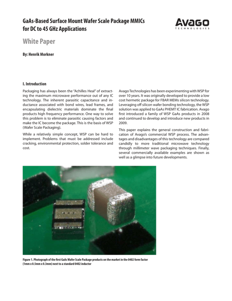
Figure 1. Photograph of the first GaAs Wafer Scale Package products on the market in the 0402 form factor
(1mm x 0.5mm x 0.3mm) next to a standard 0402 inductor
II. Basic WSP Manufacturing processes and construction
WSP starts with a standard GaAs wafer that is processed
to create a MMIC. At Avago either depletion mode or enhancement mode PHEMT wafers can be used. The wafer is
left thick, that is no vias are present, for the WSP process.
To keep yields high, wafer performance can be typically
verified with coplanar Process Control Monitor probing
before entering the WSP process.
Starting from a standard GaAs wafer, the first step in
creating a WSP is to apply a gasket material. This material
is selected for its malleability and adherence to topside
nitride and metal. Proprietary patterns and voids are made
in the gasket to ensure an air cavity forms over critical
microwave elements, such as FET fingers and transmission
lines. The height and size of the gasket and consequential
air cavities is critical since unwanted modes of microwave
propagation can form due to dielectric discontinuities
and reflections.
Figure 2. Wafer Scale Package construction and cross section
2
Once the gasket is formed another GaAs wafer, the cap,
is bonded on top. Using a GaAs wafer as the cap material
offers several advantages. It has the same thermal
expansion coefficient as the base wafer and fits into the
bonding and alignment system. It also provides a uniform
sawing medium for singulation. The actual bonding is
performed by Avago proprietary equipment built for
FBAR and GaAs wafers.
After bonding both the top side and bottom are ground
down to final package height specifications. Then a via
pattern is aligned to the bottom side to connect not only
ground but all “hot” – signal via transitions. A proprietary
metal stack is applied to the bottom side to create the
pads that can withstand a standard reflow solder process.
The bottom side metal is also patterned to relieve stress
that can form cracks.
III. Modelling and Design: WSP PCB to IC Transition
There are several physical constraints as well as electrical
issues that need to be solved in the design of the WSP
PCB to IC transition. The physical constraint is the physical
tolerance of the PCB that the WSP is mounted on. Typically,
a 100 µm gap and 200 µm pad is required for PCB to WSP
transition. The WSP must take this pad layout and transfer
the microwave energy through a relatively lossy GaAs
dielectric (DR = 12.7) up and to the inner surface. The
typical design goal is for a 50 Ω impedance (better than
-20 dB return loss) during this transition.
0
-5
-10
-15
-20
-25
-30
-35
-40
-45
-50
RL
IL
0
10
20
30
40
Frequency (GHz)
50
Figure 4. Simulated Return Loss and Insertion Loss
3
0
-1
-2
-3
-4
-5
-6
-7
-8
-9
-10
Insertion Loss (dB)
Return Loss (dB)
Figure 3. 3D Simulation Structures (HFSS) of simple thru structure
60
70
To design this transition, Avago employed several EM
simulators (HFSS and Microwave Office). EM simulation is
required due to the lack of ideal elements or traditional
transitions. Each simulator offered different advantages
and results. Differences between modelled performance is
often caused by how the boundaries and vertical dimensions are calculated as well as grid array restrictions. In the
end all results were heavily matched against measured
results. Figure 3 shows the EM simulation deck. Figure 4
shows simulated results to 60 GHz for a GaAs WSP on a
Rogers 4350 laminate PCB.
IV. Comparison to Traditional Packaging
WSP lowers parasitic loss, capacitance and inductance
WSP offers two significant advantages over conventional
microwave package technology.
WSP solutions do not have a lead frame, bond wires,
a cumbersome lid or plastic encapsulation that adds
parasitic loss, inductance, or capacitance. This gives WSP
an inherent bandwidth and high frequency performance
advantage. While most packages struggle to achieve low
loss performance above 20 GHz, WSP has demonstrated
excellent performance to 80 GHz in standard SMT and PCB
environments.
WSP simplifies the assembly process
As Figure 5 shows there are fewer steps in a WSP assembly
process. Also, these steps can be performed in a clean
automated fabrication facility. Wafers do not travel to
assembly contractors where they can be subjected to uncontrolled ESD and environmental forces.
Figure 6 shows a conventional package with its associated
loss factors.
Typical assembly processes
MMIC Wafer
Die Singulation
Die Attach Assembly
Wire bond Assembly
MMIC Wafer
Packaging Assembly
Bonded with Cap Wafer
Packaging Singulation
Figure 5a. Typical plastic package assembly process
Input Bond Wire adds Noise
and parasitic Inductance
Singulation
Figure 5b. WSP equivalent process
Plastic increases capacitance
and lower bandwidth
Output Bond Wire decreases
power and adds Inductance
MMIC wafer
RF in
Parasitic pad capacitance
decreases bandwidth
Figure 6. Typical parasitics in other SMT technologies
4
Lead frame increases
thermal resistance
RF out
V. Released–to–Market WSP product examples
The first WSP products in the market were simple. This was
necessary to keep the number of variables at a minimum
and to provide a reliable and consistent product. As with
any new technology, the goal was to build confidence and
experience. Avago introduced the VMMK-1226 e-PHEMT
FET on a 0402 (1.0 x 0.5mm) WSP in the spring of 2008.
The VMMK-1226 features DC–26 GHz performance equivalent to that of more expensive ceramic devices. The
VMMK-1226 has three leads with a complete air cavity
over the active FET. The topology is extremely simple with
no on-chip matching. Figure 7 shows the bottom leads
and inside layout.
Avago Technologies’ second generation of WSP products
use the same size and pad layout as the VMMK-1226 but
with a more complicated integrated circuit. Figure 8 shows
the VMMK-2x03 series of sub –12 GHz parts that were introduced in 2009.
Drain
Source
Gate
Parameters
Specifications
Frequency
DC – 26GHz
Operating Condition
1.5V @ 10 mA
Gain
12dB @ 12GHz
NF
0.5dB @ 12GHz
OIP3
22dBm @ 12GHz
P1dB
10dBm @ 12GHz
Figure 7. The first Avago WSP products were 200 µ and 400 µ
Float
Vdd
Size: 1.1mm x 0.6mm (0402 component)
Amp
Input
Bias-Tee
Input
Pad
Ground
Pad
50_Ohm line
Output
Output
Pad
50_Ohm line
VMMK-2103
VMMK-2203
VMMK-2303
VMMK-2403
VMMK-2503
0.5 – 6 GHz
1 – 10 GHz
0.5 – 6 GHz
2 – 4 GHz
1 – 12 GHz
Bias
5V/25mA
5V/28mA
1.8V/20mA
5V/50mA
5V/60mA
Gain
14 dB
16 dB
13 dB
15 dB
14 dB
NF
2.4 dB
2.3 dB
< 2.5 dB
2.5 dB
3.7 dB
OIP3
23 dBm
15 dBm
23 dBm
32 dBm
28 dBm
P1dB
NA
NA
10 dBm
20 dBm
17 dBm
Freq Range
Figure 8. 2009 Avago second generation WSP introductions
5
Bias-Tee
VI. WSP applications and simulation
Avago WSP products in the 0402 format are intended to
be basic building blocks in a variety of systems. While
there certainly are military applications (small size and a
near hermetic package) the main targets are commercial
and consumer applications such as DBS satellite, GPS and
radar detectors.
One of the challenges to wide WSP use involves simulation and performance verification. Avago has dedicated
much effort to this. Avago now provides both traditional sparameter and x-parameter data. The x-parameters follow
a new standard introduced by Agilent. Additional information is available at: (http://www.home.agilent.com/
agilent/application.jspx?nid=-34017.0.00&US&lc=eng)
Figure 9 shows an example WSP application along with
x-parameter data.
Avago WSP application with x–parameters
The advantages and key features of x-parameters are
widely quoted:
“X-parameters can help you overcome a key challenge in
RF engineering, namely that nonlinear impedance differences, harmonic mixing, and nonlinear reflection effects that
occur when components are cascaded under large signal
operating conditions. This means that there is a nonlinear,
and as such, non-trivial relationship between the properties
of the individual cascaded components and the composite
properties of the resulting cascade. This situation is unlike
that at DC; where one can (for example), simply add the
values of resistors connected in series. X-parameters help
solve this cascading problem: if you measure the X-parameters of a set of components individually, you can calculate
the X-parameters and hence the nonlinear transfer function
of any cascade made from them1.”
40
20
0
-20
-40
-60
-80
-100
-120
-140
Figure 9 a. A 0402 VMMK part mounted on a PCB
dBm(Vout[::,1])
dBm(Vout[::,5])
dBm(Vout[::,4])
dBm(Vout[::,3])
dBm(Vout[::,2])
-20 -18 -16 -14 -12 -10 -8 -6 -4 -2 0
Pin
2
4
6
8 10 12
Figure 9 b. 1st, 2nd, 3rd, 4th, and 5th Harmonic from x-par
Vdd
0.1uF
Graphical Extrapolation of the IP3 Point
60
40
100pF
20
Size: 1.1mm x 0.6mm (0402 component)
0
-20
Input
Input
Pad
Ground
Pad
-40
Output
Amp
-60
Output
Pad
50_Ohm line
Figure 9 c. Typical VMMK bias network
-80
Bias-Tee
-100
50_Ohm line
-25
-20
-15
-10
-5
0
5
extended_range
10
15
20
25
1.5
2.0
2.5
Figure 9 d. Output IP3 as calculated using x-parameters
Transmitted Spectrum
0
Spectrum_in
Spectrum_out
-20
-40
-60
-80
-100
-120
Figure 9 e. Typical VMMK demonstration board
6
-2.5
-2.0
-1.5
-1.0
-0.5 0.0 0.5
freq, MHz
Figure 9 f. ACPR as calculated using x-parameters
1.0
VII. Conclusion and future developments
WSP technology as implemented at Avago Technologies
provides a viable and reliable solution to future microwave
through millimeter needs. It has better performance than
traditional packaging by eliminating bond wires, lead
frames, and laminate or plastic encapsulates. It provides a
complete sealed environment (passing MSL level 2) for the
active components yet provides a low dielectric constant
(air) cavity above the chip. Users find assembly is easy and
as volume increases existing automation equipment will
drive their costs lower.
The WSP starts as a standard processed GaAs wafer. The
backside vias and I/O pads serve as the lead-frame of the
wafer scale package. The backside metal is thick enough
to ensure adequate coverage in the bottom of the vias
without inhibiting the use of standard solder paste in
assembly. The pad size and separation are adequate to
ensure that no special package footprint concessions
need to be made by customers and their board houses.
Lead-free solder paste is the recommended adhesive, as it
will help the parts self-align on the board.
There are some drawbacks to this technology. The first
is that GaAs is inherently fragile, thus the metal backing
of the WSP must be carefully controlled to prevent stress
cracks during application. Secondly, the die is inherently
larger in a WSP application versus a pure chip and wire
assembly. Real estate wise it is more expensive.
Figure 10. Prototype WSP 3 x 3mm DC–50GHz TWA
7
The largest hurdle to wide customer adoption is that the
technology is new. Most microwave through millimeter
wave IC users are conservative and slow to adopt new
ideas into their mainstream manufacturing. The need for
compact solutions and better performance are strong
driving forces that counter this conservatism.
Development continues at Avago to expand and diversify
the WSP portfolio. In 2009 there will many new products
released to market using the 0402 format to make basic
microwave building blocks, including amplifiers, detectors,
switches and mixers. Also during 2009, sampling and reliability qualification will start on larger package formats
that allow more functions. This will include 1 x 2 mm, 2 x
2 mm, and 3 x 3 mm packages with QFN compatible footprints. These new products will have heights of only 0.4
mm. Applications for the more complex and larger WSP
products include Ka and Ku band 2 W power amplifiers,
38 GHz down-converters and up-converters, and e-band
products. Figure 10 shows a prototype DC–50 GHz TWA in
a 3 x 3 mm WSP.
Design and construction of GaAs based WSP is relatively
straightforward once certain hurdles are passed. The
fabrication hurdle is to bond two wafers together while
forming a perfect air gap over critical active areas of the IC.
The design hurdle is to properly model the 3-dimension
transitions with minimal parasitic losses or unwanted
mode creation. The last hurdle is customer adoption and
usage, which requires applications where the advantages
of WSP far outweigh any risks.
References
[1] K. Phan, J. Kessler, H. Morkner, M. Vice, L. Nguyen, J. Roland, “A Miniaturized Wafer-Scale Package Demonstrated
with Three Enhancement Mode Amplifiers”, EuMC 2008, October 2008
[2] S. Kumar, J. Kessler, H. Morkner, ”6-24 GHz Mixer Using 0.25um Enhancement Mode PHEMT Technology in a Low
Cost Chip Scale Package”, EuMC 2008, October 2008
[3] K. Phan, H Morkner, “A High Performance Yet Easy to Use Low Noise Amplifier in SMT Package for 6 to 20GHz Low
Cost Applications,” European Microwave Conference, 12th GaAs Symposium, Amsterdam pp. 603-606, 2004.
[4] K. Phan, K. Fujii, H. Morker, “Two High Dynamic Range mmW Amplifiers in SMT Package with ESD Protection,“ 37th
European Microwave Conference, Munich, pp. 1209-1212, 2007
[5] K. Kobayashi, “Improved Efficiency, IP3-Bandwidth and Robustness of a Microwave Darlington Amplifier using
0.5um ED PHEMT and a New Circuit Topology,” IEEE CSIC Digest, pp. 93-96, 2005
[6] S. Kumar, M. Vice, H. Morkner, W. Lam, “Enhancement mode GaAs PHEMT LNA with linearity Control (IP3) and Phase
matched Mitigated Bypass Switch with Differential Active Mixer,” IEEE 2003 International Microwave Symposium,
[7] H. Morkner, M. Frank, S. Yajima, “A Miniature PHEMT Switched-LNA for 800MHz to 8 GHz Handset Applications”,
IEEE 1999 RFIC Symposium, June 1999, Session TUE1-2
1 Agilent Technologies.
For product information and a complete list of distributors, please go to our web site:
www.avagotech.com
Avago, Avago Technologies, and the A logo are trademarks of Avago Technologies in the United States and other countries.
Data subject to change. Copyright © 2005-2009 Avago Technologies. All rights reserved.
AV02-2103EN - September 16, 2009
