simple bi-directional dc-to-dc converters with high input to output
advertisement
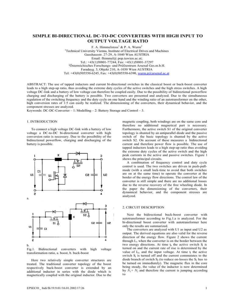
SIMPLE BI-DIRECTIONAL DC-TO-DC CONVERTERS WITH HIGH INPUT TO OUTPUT VOLTAGE RATIO F. A. Himmelstoss1 & P. A. Wurm2 Technical University Vienna, Institute of Electrical Drives and Machines Gusshausstr. 27-29, A-1040 Wien AUSTRIA Email: fhimmel@ pop.tuwien.ac.at; Tel.: +43(1)58801-77244, Fax: +43(1)58801-37297 2 Österreichisches Forschungs- und Prüfzentrum Arsenal Ges.m.b.H. Faradayg. 3, Objekt 210, A-1030 Wien AUSTRIA Tel: +43(0)505550-6245, Fax: +43(0)505550-6390, wurm.p@arsenal.ac.at 1 ABSTRACT: The use of tapped inductors and current bi-directional switches in the classical boost or buck-boost converter leads to a high step-up ratio, thus avoiding the extreme duty cycles of the active switches and the high stress switches. A high voltage DC-link and a battery of low voltage can therefore be coupled easily. Due to the possibility of bidirectional powerflow charging and discharging of the battery is possible. Two converters are presented and analyzed. Due to the simultaneous regulation of the switching frequency and the duty cycle on one hand and the winding ratio of an autotransformer on the other, high conversion rates of 1:5 can easily be realized. The dimensioning of the converters, their dynamical behavior, and the component stresses are analyzed. Keywords: DC-DC-Converter – 1: Modelling – 2: Battery Storage and Control – 3. 1. INTRODUCTION To connect a high voltage DC-link with a battery of low voltage a DC-to-DC bi-directional converter with high conversion ratio is necessary. Due to the possibility of the bidirectional powerflow, charging and discharging of the battery is possible. a. magnetic coupling, both windings are on the same core and therefore no additional magnetical part is necessary. Furthermore, the active switch S1 of the original converter topology is shunted by an antiparallel diode and the passive switch of the basic topology is shunted by the active switch S2. On account of these measures a bidirectional current and therefore power flow is possible. The use of tapped inductors leads to a high step-up ratio thus avoiding the extreme duty cycles of the active switch and the high peak currents in the active and passive switches. Figure 1 shows the principal circuits. A combination of frequency control and duty cycle control is used. The two switches are driven in push-pullmode (with a small lock-time to avoid that both switches are on at the same time) to operate the converter at the border of the energy flow directions. The control law of the converter is still simple and there are no additional losses due to the reverse recovery of the free wheeling diode. In the paper the dimensioning of the converters, their dynamical behavior, and the component stresses are analyzed. 2. CIRCUIT DESCRIPTION b. Fig.1. Bidirectional converters with high transformation ratio, a. boost, b. buck-boost voltage Here two relatively simple converter structures are treated. The traditional converter topology of the boost respectively buck-boost converter is extended by an additional inductor in series with the diode which is magnetically coupled with the original inductor. Due to the EPSEC01_ bidi/fh/19.9.01//16.01.2002/17:26 Next the bidirectional buck-boost converter with autotransformer according to Fig.1.a is analyzed. For the bi-directional boost converter with autotransformer here only the results are summarized. The converters are analyzed with U1 as input and U2 as output. The derived equations are also valid for the reverse direction of the energy flow. Figure 2 shows the current through L1 when the converter is on the border between the two energy directions. At time t0 the active switch S1 is turned on and the current rate of rise is determined by the value of L1, and the input voltage. At time t1 the active switch S1 is turned off and the current commutates to the diode branch of switch S2 (to reduce on-losses the S2 has to be turned on immediately). The magnetic flux in the core being steady, the value of the inductor is now determined by N1+ N2 and therefore the current is jumping according to 1 I S 2P = I S1P ⋅ N1 N1 + N 2 (1) where IS2P stands for the peak current through switch S2 and IS1P for the peak current through switch S1. The current decreases according to the output voltage and the inductor value N + N2 Lgen = 1 N2 2 ⋅ L1 = n 2 ⋅ L1 . (2) between the two energy directions in normalized form according to f 1 = (5) f B 2 ⋅ (n + M )2 with R fB = L (6) L1 and displayed in Fig.4. f/fB 0.1 0.05 n=1 n=4 0 1 2 3 M 4 5 Fig.4.a. Buck-boost: switching frequency The energy stored in L1 at time t1 is completely transferred to the output at t2 (if the converter is at the border between the two energy directions). For the continuous mode (and a bi-directional is normally in the continuous mode of operation) it is easy to calculate the voltage transfer ratio M according to U d ⋅n M = 2 = (3) U1 (1 − d ) with the winding ratio N + N2 n= 1 . (4) N2 By setting n = 1 one gets the well-known transfer ratio of the classical buck/boost converter. Figure 3 shows the dependence of the output to input voltage ratio M according to the duty cycle d for different winding ratios n. One can see that for the same duty cycle much lower voltage transformation rates can be obtained. 8 n=4 M 4 n=1 2 0 0.2 0.4 15 n=1 10 5 n=4 0 5 10 15 M Fig.5. Buck-boost: voltage stress (active switch) The average currents of the diode I D and the switch I S normalized to the load current are IS 2 =1 (9) I Load 10 6 U S 2P =n+M . (8) U1 Figure 5 shows a decrease of the voltage stress of the active switch and an increase of the voltage stress of the diode when the winding ratio is increased. U1sp/U1 Fig.2. upper trace (Ch2): Current through L1 (0.1A/div), lower trace (Ch3): gate-source voltage The voltage stress of the active switch US1 and the active switch US2 is given normalized to the input voltage by U S 1P M =1 + (7) U1 n 0.6 0.8 1 d Fig.3.a. Buck-boost: voltage transfer ratio The switching frequency can be calculated for constant input voltage and constant output power for the border EPSEC01_ bidi/fh/19.9.01//16.01.2002/17:26 I S1 =M . (10) I Load For the selection of the power devices, however, also the peak pulse currents are important. With U2 d= (11) (n ⋅ U 1 + U 2 ) one can calculate the peak current through switch S2 IS2P I S2S (n + M ) . = 2⋅ (12) I Load n 2 For the switched model of the converter the transients of the switches are neglected, but the parasitic resistances are included; they are the resistance of the switch rS1, of the switch rS2 of the winding parts rL1 and rL2, and the series resistance of the output capacitor rC. Due to the push-pull mode of the switches, the diodes are shunted and the forward voltage of the diodes can be omitted. One can establish three describing differential equation systems depending on which electronical switch is closed or open. For using the converter only in the continuous mode, an averaged model of the circuit is very useful (it needs less computation time). In this case the converter can be described by d λ a11 a12 λ = ⋅ + A⋅ u 1 (15) dt u C a 21 a 22 u C with the state variables flux linkage λ and voltage across the output capacitor and with the elements of the system matrix according to r +r 1 a11 = − L1 S1 ⋅ d + − 2 ⋅ ((rS 2 + rL2 + rL2) + RL // rC ) ⋅ (1− d) (16) L n ⋅ L 1 1 RL ⋅ (1 − d ) a12 = − (17) R + rC L RL ⋅ (1 − d ) a2 1 = 2 (18) n ⋅ L 1 ⋅ C ⋅ ( R L + rC ) 1 a22 = − C ⋅ (R L + rC ) and the input vector d A= . (20) 0 The input current is now described by N i1 = 1 ⋅ d ⋅ λ . (21) L1 The duty cycle d is used as weighting factor leading to a nonlinear differential equation. It can also be interpreted as a switching function which is one when the active switch S1 is turned on and zero when the active switch S1 is turned off (consequently the active switch S2 was turned on). The given model is nonlinear due to the multiplication of the duty cycle with the state variables. EPSEC01_ bidi/fh/19.9.01//16.01.2002/17:26 Here the important equations for the autotransformer boost converter are summarized. The calculation can be done similarly according to chapters 2 and 3. Equations (1, 2, 4, 6, 14) are the same. The transfer ratio M is U 1 + d ⋅ (n − 1) M = 2 = , (22) U1 (1 − d ) the normalized switching frequency for the border between energy direction f M −1 = , (23) f B 2 ⋅ M ⋅ (M + (n − 1))2 the maximum voltage across the switch US 1 = ⋅ (M + n − 1) , (24) U1 n the maximum voltage across the diode UD = M + n −1 , (25) U1 the maximum peak current through the switch ISP = 2 ⋅ ( M + n − 1) , (26) I Load the maximum current through the diode I DP M + n −1 = 2⋅ , (27) I Load n the maximum switching power of the active and the passive switch PDP P (M + n − 1)2 . = SP = 2 ⋅ (28) PB PB n 15 12 9 n=4 M 3. DYNAMICAL MODEL 4. EQUATION SURVEY FOR THE AUTOTRANSFORMER BI-DIRECTIONAL BOOST CONVERTER 6 3 0 n=1 0 0.2 0.4 0.6 0.8 1 d (19) Fig.6. Boost: voltage transfer ratio n=1 0.1 f/fB We define the switching power of the switch S2 PS2P by multiplying the peak current Eq.(10) with the maximum voltage Eq.(7).The peak switching power of the active and the passive switch are the same. In normalized form one can write PS 1 P PS 2 P (n + M )2 = = 2⋅ (13) PB PB n with PB = I Load ⋅ U 1 . (14) For higher winding ratios, the switching power decreases significantly (M higher then two) for small input voltages and increases for higher input voltages. 0.05 n=4 0 1 2 3 M 4 5 Fig.7. Boost: switching frequency 3 If the converter is operated in push-pull mode in such a way that the energy direction is changing in each switching period, a low loss zero current switching can be obtained. In this case only small capacitors have to be connected in parallel to the switches. Both switches can now turn on and off at zero voltage and switching losses can be avoided. U1sp/U1 15 n=1 10 5 CONCLUSIONS n=4 0 5 10 15 M Fig.8. Boost: voltage stress (active switch) The Figures show the voltage transformation ratio (Fig.6) over duty ratio, the normalized frequency (Fig.7), and the normalized switch voltage (Fig.8), with the winding ratio n as parameter. Figures 7 and 8 use the voltage conversion ratio M as an independent variable. The dynamics of the converter can be described again with Eq.(15). From the dynamics point of view there are only little differences. Only the input vector has to be changed to 1 A= . (29) 0 The dimensioning of the bidirectional boost and the buckboost converter with tapped inductor (autotransformer), the component stresses, and the dynamical behavior were treated. Using a combined frequency and duty cycle control leads to a better utilization of the semiconductor devices and reduced losses due to the possibility to use the border between the two energy directions. The frequency range of the converter decreases with increasing winding ratio n and the position of the frequency range can be adjusted by L1. Reducing component stress of the semiconductor devices reduces their costs. Due to the simultaneous regulation of the switching frequency and the duty cycle in combination with the autotransformer, the component stresses can be reduced and a very high step-up ratio of 5:1 can easily be reached. ACKNOWLEDGEMENT 5. CONVERTER CONTROL There are different methods to control the converter. The traditional way is to use a fixed frequency and to vary the duty cycle. Operating a bidirectional converter with fixed frequency at low load leads to an oscillation of energy between the two sides of the converter. The current ripple through the inductor is the same independent of the load, because it only depends on the voltage levels (source voltage, load voltage) of the converter. In the case of low load this leads to on-state losses and additional switching losses. To reduce these losses a frequency control according to (5) for the buck-boost and according to (23) for the boost converter was proposed. The frequency increases when the load decreases. For higher loads the frequency decreases but the peak current increases leading to higher on-state losses. The leading switch (in the description used in this paper this is S1) always turns on with zero current condition and turns off under hard switching condition. For the other switch the opposite is true. The turn-on losses due to the output capacitor of the leading switch are proportional to the switching frequency. For very low load it is therefore reasonable to use a quasi discontinuous mode. The switches are not driven in push-pull but in single switch mode. Depending on the used energy direction only, one switch is pulsed. The other is completely blocked. The current is commutated into the parallel diode of the blocked active switch which acts now as a simple freewheeling diode. The higher losses of the diode compared to an active switch are insignificant in this case. EPSEC01_ bidi/fh/19.9.01//16.01.2002/17:26 The first author is very much indebted to the “ Fonds der wissenschaftlichen Forschung FWF” which supports the work of the Power Electronics Section at their university. 7. REFERENCES [1] [2] [3] [4] [5] [6] [7] R.D.Middlebrook, ”A Continuous Model for the Tapped-Inductor Boost Converter,” IEEE PESC 1975 Record, pp.63 M.Rico, J.Uceda, J.Sebastian, & F.Aldana, ”Static and Dynamic Modeling of Tapped-Inductor DC-toDC Converters,” IEEE PESC 1987 Record, pp.281288. J.Sebastian, J.Uceda, M.A.Perez, M.Rico, & F.Aldana, ”A Very Simple Method to Obtain One Additional Fully Regulated Output in Zero-CurrentSwitched Quasiresonant -79. Converters, ” IEEE PESC 1990 Record, pp.536-542. M.Brown, ”Very Wide Input Range, Flyback PWM Switching Power Supply,” Proc. of HFPC’94, San Jose, Ca., pp.163-172. L.L.Erhartt & F.A.Himmelstoss, ”A Simple BoostConverter with High Step-Up Ratio, ” in Proc. of PCIM’95, pp. 433-441. P.H.Wurm., & F.A.Himmelstoss, ”Application of EXCEL for Analyzing DC/DC Converters, ” 6th Workshop on Computer in Power Electronics COMPEL, Como (1998) F.A.Himmelstoss, & P.H.Wurm, ”Simple Converters with High Step-Down Conversion Ratio,” PCIM’99, June 1999. 4
