1300 Henley Court
Pullman, WA 99163
509.334.6306
www.digilentinc.com
PmodDA1™ Reference Manual
Revised May 24, 2016
This manual applies to the PmodDA1 rev. C
Overview
The Digilent PmodDA1 is an 8-bit Digital-to-Analog Converter module that can output up to four different analog
signals simultaneously. This module is ideal for users who want to output a variable voltage signal but do not want
to use up their system board's analog capable pins.
Features include:
Two 8-bit DACs
Four D/A conversion channels
Maximum conversion rate of 1.875 MSa
Small PCB size for flexible designs 1.0“ ×
0.8” (2.5 cm × 2.0 cm)
6-pin Pmod connector with GPIO interface
Library and example code available
in resource center
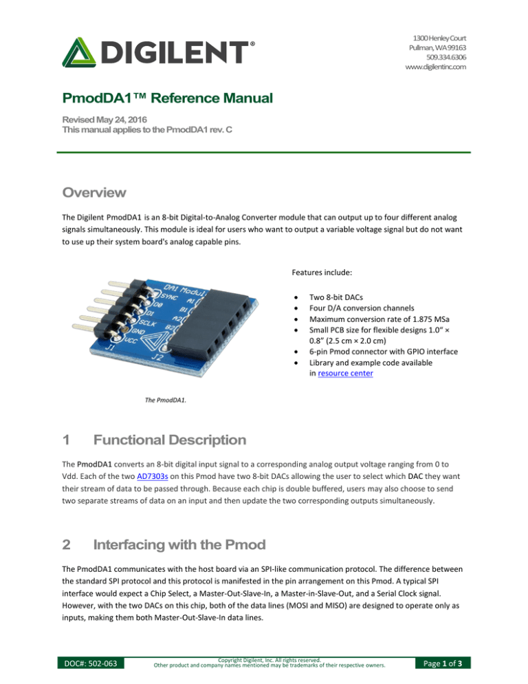
The PmodDA1.
1
Functional Description
The PmodDA1 converts an 8-bit digital input signal to a corresponding analog output voltage ranging from 0 to
Vdd. Each of the two AD7303s on this Pmod have two 8-bit DACs allowing the user to select which DAC they want
their stream of data to be passed through. Because each chip is double buffered, users may also choose to send
two separate streams of data on an input and then update the two corresponding outputs simultaneously.
2
Interfacing with the Pmod
The PmodDA1 communicates with the host board via an SPI-like communication protocol. The difference between
the standard SPI protocol and this protocol is manifested in the pin arrangement on this Pmod. A typical SPI
interface would expect a Chip Select, a Master-Out-Slave-In, a Master-in-Slave-Out, and a Serial Clock signal.
However, with the two DACs on this chip, both of the data lines (MOSI and MISO) are designed to operate only as
inputs, making them both Master-Out-Slave-In data lines.
DOC#: 502-063
Copyright Digilent, Inc. All rights reserved.
Other product and company names mentioned may be trademarks of their respective owners.
Page 1 of 3
PmodDA1™ Reference Manual
The PmodDA1 will receive its 8 bits of information from the system board through 16 clock cycles with first eight
bits consisting of eight control bits and the remaining eight bits representing the 8 bits of the data with the MSB
first. Each bit is received by the rising edge of the serial clock line. The function dictated by the first eight control
bits is executed when the chip select line is brought high.
A pinout table and diagram for the PmodDA1 are provided below:
Header J1
Pin
Signal
Description
1
~SYNC
Chip Select (active low)
2
D0
Input Data 1
3
D1
Input Data 2
4
SCK
Serial Clock
5
GND
Power Supply Ground
6
VCC
Power Supply (3.3V/5V)
Header J2
Pin
Signal
Description
1
A1
Output Data A1
2
B1
Output Data B1
3
A2
Output Data A2
4
B2
Output Data B2
5
GND
Power Supply Ground
6
VCC
Positive Power Supply
Figure 1. PmodDA1 circuit diagram.
Table 1. Connector J1: Pin descriptions as labeled on the Pmod.
The on-board DACs can in principle use either an external or internal reference voltage; however, the PmodDA1 is
designed that the internal reference voltage of Vdd/2 volts must be used. Because of this, the first bit in the
command signal sent to the Pmod must always be a logic low signal in order to use the internal reference voltage
on the DAC. Tables describing the command signal and the associated bits from the AD7303 datasheet are
provided below.
~INT/EXT
X
Control Bits
LDAC PDB PDA
(MSB)
~A/B
CR1
CR0
DB7
DB6
DB5
Data Bits
DB4 DB3
(LSB)
DB2
DB1
Table 2. PmodDA1 input shift register structure.
Note: The "~" signifies that the signal is active when driven low.
Copyright Digilent, Inc. All rights reserved.
Other product and company names mentioned may be trademarks of their respective owners.
Page 2 of 3
DB0
PmodDA1™ Reference Manual
Bite Name
~INT/EXT
X
LDAC
PDB
PDA
~A/B
CR1
CR0
Data
Description
Selects between the internal and external voltage reference
Don't care
Load DAC bit to both load and update the DAC outputs
Power-down DAC B
Power-down DAC A
Selects either DAC A or DAC B to process the data
Works with CR0 as per the Control Bits Truth Table below
Works with CR1 as per the Control Bits Truth Table below
The user submitted data where DB7 is the MSB and DB0 is the LSB
Table 3. Bit descriptions.
LDAC
0
0
0
0
0
0
0
~A/B
X
0
1
0
1
0
1
CR1
0
0
0
1
1
1
1
CR0
0
1
1
0
0
1
1
1
0
X
X
1
1
X
X
Resulting Operation
Both DAC registers loaded from the shift register
Update DAC A register from the shift register
Update DAC B register from the shift register
Update DAC A DAC register from the input register
Update DAC B DAC register from the input register
Update DAC A DAC register from the shift register
Update DAC B DAC register from the shift register
Load DAC A input register from the shift register and update both DAC
registers
Load DAC B input register from the shift register and update both DAC
registers
Table 4. Control bits truth table.
PDA
0
PDB
0
0
1
1
0
1
~INT/EXT
0
1
1
Description
Internal Vdd/2 reference
voltage selected
External reference voltage
selected
Description
Both DACs are active
DAC A is active and DAC B is in powerdown mode
DAC B is active and DAC is in powerdown mode
Both DACs are in power-down mode
Table 5. Another truth table compiled from the AD7303 datasheet.
3
Physical Dimensions
The pins on the pin header are spaced 100 mil apart. The PCB is 1 inch long on the sides parallel to the pins on the
pin header and 0.8 inches long on the sides perpendicular to the pin header.
Copyright Digilent, Inc. All rights reserved.
Other product and company names mentioned may be trademarks of their respective owners.
Page 3 of 3

