HSMP-3816
Quad PIN Diode π Attenuator 300 kHz to 4 GHz
in SOT 25 Package
Data Sheet
Description
Features
Avago Technologies’ HSMP-3816 is a wideband, low
insertion loss, high IIP3, Quad PIN Attenuator in a low cost
surface mount SOT-25 package. It provides a good match
and flat attenuation over an extremely wide band from
300 kHz to 4 GHz.
• 4 PIN Diodes in a SOT-25 package
The SOT-25 packages gives a reduction in part count and
takes up less space on board compared to multi package
solutions.
• MSL-1 and Lead-free
• 300 kHz to 4 GHz usable frequency band
• High Linearity
• Low insertion Loss
• Tape & Reel packaging option available
Four PIN Diodes in one package encourages performance
repeatability for improved production yield at board
level.
Specification At 1 GHz, V+=5V
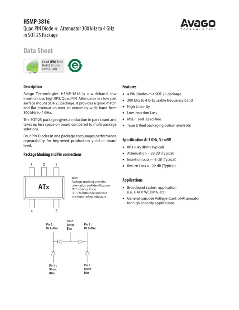
Package Marking and Pin connections
• Attenuation = 38 dB (Typical)
3
2
4
• Insertion Loss = -3 dB (Typical)
1
• Return Loss = - 22 dB (Typical)
Note:
Package marking provides
orientation and identification
“AT”= Device Code
“x” = Month code indicates
the month of manufacture
ATx
5
Pin 3 :
RF In/Out
Pin 4 :
Shunt
Bias
• IIP3 = 45 dBm (Typical)
Pin 2 :
Series
Bias
Pin 1 :
RF In/Out
Pin 5 :
Shunt
Bias
Applications
• Broadband system application
(i.e., CATV, WCDMA, etc)
• General purpose Voltage-Control-Attenuator
for high linearity applications.
Absolute Max Ratings [1], Tc = +25oC
Symbol
Parameter
Unit
Abs Max
If
Forward Current (1 µs Pulse)
Amp
1
PIV
Peak Inverse Voltage
V
100
Tj
Junction Temperature
°C
150
Tstg
Storage Temperature
°C
-60 to 150
qlb
Thermal Resistance [2]
°C/W
167
PIn
Input Power [3]
W
1.0
Notes:
1. Operation in excess of any one of these conditions may result in permanent damage to the device.
2. Thermal Resistance is measured from junction to board using IR method.
3. The Max Input Power is tested using demoboard as shown in Figure 1 at the worst-case (highest attenuation) bias condition of V+=5V, Vc=0V.
Electrical Specifications, Tc = +25oC (Each Diode)
Test
Conditions
Minimum
Breakdown
Voltage
VBR (V)
Maximum
Total
Capacitance
CT (pF)
Minimum
Resistance
at IF = 0.01mA,
RH (Ω)
Maximum
Resistance
at IF = 20mA,
RL (Ω)
Maximum
Resistance
at IF = 100mA,
RT (Ω)
Resistance
at IF = 1mA,
RM (Ω)
100
0.35
1500
10
3.0
45 to 80
VR = VBR Measure
IR≤ 10uA
VR = 50V
f = 1MHz
IF = 0.01mA
f = 100MHz
IF = 20mA
f = 100MHz
IF = 100mA
f = 100MHz
IF = 1mA
f = 100MHz
Note : Rs parameters are tested under AQL 1.0
Typical Performance, Tc = +25oC (Each Diode)
Test
Condition
Carrier Lifetime
t(ns)
Reverse Recovery Time
Trr (ns)
Total Capacitance
CT (pF)
1500
300
0.27
IF = 50mA
IR = 250 mA
VR = 10 V
IF = 20 mA
90% Recovery
VR = 50V
f = 1MHz
Typical Performance for HSMP-3816 Quad PIN Diode π Attenuator @ +25oC
Parameter
Test Condition
Units
Typical
Insertion Loss
Vc = 15V, V+ = 5V, Freq = 1GHz
dB
-3.0
Return Loss
Vc = 0V, V+ = 5V, Freq = 1GHz
dB
-22
Attenuation
Vc = 0V, V+ = 5V, Freq = 1GHz
dB
38
Input IP3
Vc = 1.5V, V+ = 5V, Freq = 1GHz
dBm
45
Input IP3
Vc = 15V, V+ = 5V, Freq = 1GHz
dBm
42
Input IP3
Vc = 1.5V, V+ = 5V, Freq = 100MHz
dBm
37
Input IP3
Vc = 15V, V+ = 5V, Freq = 100MHz
dBm
37
Input IP3
Vc = 1.5V, V+ = 5V, Freq = 30MHz
dBm
35
Input IP3
Vc = 15V, V+ = 5V, Freq = 30MHz
dBm
35
Notes :
1. Measurement above obtained using Wideband RF circuit design shown in Figure 1 & 2
C3
R3
Iseries
HSMP-3816
C1
Typical Performance Curves for Single Diode@ Tc = +25oC,
Vc
10000
C2
In/Out
RF Resistance (OHMS)
In/Out
Ishunt
R1
R2
R4
R4
R5
C4
C5
V+
TA = +85˚C
TA = +25˚C
TA = - 55˚C
1000
100
10
1
0.01
Figure 1. Wideband Quad PIN Diode π Attenuator Circuit
Figure 3. RF Resistance vs. Forward Bias Current
Vc
100.00
C3
R3
C1
Via Hole
to GND
R1
R2
ATx
C4
C2
IF - Forward Current (mA)
Via Hole
to GND
C5
R4
R4
R5
100.00
0.10
1.00
10.00
IF - Forward Bias Current (mA)
10.00
1.00
0.10
0.01
Via Hole
to GND
+125°C
0
0.2
+25°C
- 50°C
0.4
0.6
0.8
VF- Forward Voltage (V)
1
1.2
Figure 4. Forward Current vs. Forward Voltage
V+
Figure 2. Circuit Board Layout
0.60
Value
R1,R2
560 Ohm
R3
330 Ohm
R4
1500 Ohm
R5
680 Ohm
C1-C5
47000 pF
0.55
Total Capacitance (pF)
Component
0.50
0.45
0.40
0.35
0.30
F=1 MHz
0.25
F=10 MHz
0.20
0.15
0
4
8
12
Reverse Voltage (V)
Figure 5. RF Capacitance vs Reverse Bias
16
20
Typical Performance Curves for HSMP-3816, @ V+ = 5V, Tc = +25oC
100
60
40
Insertion Loss (dB)
F = 1 GHz
20
Attenuation (dB)
0
Vc=15V
-10
6.0
F = 10 MHz
F = 100 MHz
F = 3 GHz
10
1
Control Voltage Vc (Volts)
10
1.7
-40
-10
45
100
Frequency (MHz)
1000
IP3 - Input (dBm)
F = 1 GHz
-20
Vc=0V
-30
Vc=15V
-40
40
F = 100 MHz
F = 30 MHz
35
30
25
100
Frequency (MHz)
20
1000
16
2
1.8
14
1.6
I series
1.4
1.2
10
1
8
0.8
6
0.6
4
0.4
2
I shunt
0
5
10
15
Control Voltage Vc (Volts)
20
Figure 10. Series & Shunt Diode Bias Current vs. Control Voltage
0.2
0
Shunt Diode Bias Current - Ishunt (mA)
18
12
0
2
4
6
8
10 12 14
Vc - Control Voltage (V)
16
18 20
Figure 9. Input IIP3 vs. Control Voltage
45
Vc=0V
1.1V
1.3V
40
35
30
Attenuation (dB)
10
Figure 8. Return Loss vs. Frequency
Series Diode Bias Current - Iseries (mA)
Vc=0V
Figure 7. Insertion Loss vs. Frequency
50
0
1.1
-70
0
-50
1.3
1.17
-50
-60
10
Figure 6. Attenuation vs. Control Voltage
Return Loss (dB)
2.4
-30
-80
-90
-100
1
0
-20
1.7V
25
20
2.4V
15
10
6V
5
0
-40
15V
-20
0
20
40
Temp (Degree C)
60
80
Figure 11. Attenuation vs. Temperature
Note:
1. Measurements above were obtained using Wideband RF circuit design shown in Figures 1 and 2.
2. Typical values were derived using limited samples during initial product characterization and may not be representative of the overall distribution.
Package Outline & Dimension
D
Dimension
E
H
B
e
e1
L2
CL
PKG
A2
A
0.250
A1
SEATING
PLANE
L
GAGE PLANE
PCB Footprint
0.074
1.9
0.037
0.95
0.094
2.4
0.039
1.0
0.028
0.7
DIMENSIONS IN
Inches
mm
C
Symbol
Minimum
Nominal
Maximum
D
2.80
2.90
3.00
H
2.60
2.80
3.00
E
1.50
1.60
1.70
e1
1.88
1.90
1.92
e
0.93
0.95
0.97
B
0.35
0.50
A2
0.9
C
0.08
1.15
1.30
0.22
L
0.35
0.60
A1
0
0.15
A
0.9
1.40
Device Orientation
Top View
REEL
4 mm
End View
CARRIER
8 mm
TAPE
ATx
USER
FEED
DIRECTION
ATx
ATx
ATx
COVER TAPE
Tape Dimension
D
Po
P2
E
T1
Bo
W
F
7˚ MAX
Ao
P
Ko
D1
8˚ MAX
Milmeters
Symbol
Nominal
Minimum
Maximum
V
8.00 (0.315)
7.90 (0.311)
8.30 (0.327)
P
4.00 (0.157)
3.90 (0.154)
4.10 (0.161)
E
1.75 (0.069)
1.65 (0.065)
1.85 (0.073)
F
3.50 (0.138)
3.45 (0.136)
3.55 (0.140)
J
1.50 (0.059)
N/A
1.60 (0.063)
J1
1.00 (0.039)
N/A
Po
4.00 (0.157)
Part Number Ordering Information
Part number
No. of Units
Container
1.25 (0.049)
HSMP-3816-BLKG
100
Anti-static bag
3.90 (0.154)
4.10 (0.161)
HSMP-3816-TR1G
3000
7” reel
HSMP-3816-TR2G
10000
13” reel
P2
2.00 (0.079)
1.95 (0.077)
2.05 (0.081)
Ao
3.23 (0.127)
3.13 (0.123)
3.33 (0.131)
Jo
3.81 (0.125)
3.08 (0.121)
3.28 (0.129)
Fo
1.60(0.063)
1.50 (0.059)
1.70 (0.067)
T1
0.257 (0.0100)
0.241 (0.0095)
0.267 (0.0105)
For product information and a complete list of distributors, please go to our web site: www.avagotech.com
Avago, Avago Technologies, and the A logo are trademarks of Avago Technologies in the United States and other countries.
Data subject to change. Copyright © 2005-2009 Avago Technologies. All rights reserved. Obsoletes AV01-0066EN
AV02-0407EN - June 3, 2009
