Datasheet - SHF Communication Technologies AG
advertisement

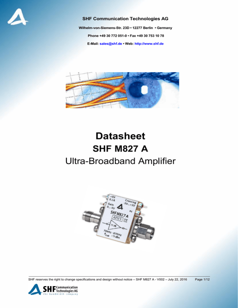
SHF Communication Technologies AG Wilhelm-von-Siemens-Str. 23D • 12277 Berlin • Germany Phone +49 30 772 051-0 • Fax +49 30 753 10 78 E-Mail: sales@shf.de • Web: http://www.shf.de Datasheet SHF M827 A Ultra-Broadband Amplifier SHF reserves the right to change specifications and design without notice – SHF M827 A - V002 – July 22, 2016 Page 1/12 Description The SHF M827 A is an ultra-broadband RF amplifier with a small footprint and a bandwidth of more than 67 GHz. It is the improved successor to the popular SHF 827 linear driver amplifier. A single stage amplifier design is employed using our monolithic microwave integrated circuit (MMIC) inside special carriers to achieve the ultra-wide bandwidth and the low noise performance. This extreme bandwidth offers the capability to amplify binary signals of more than 100 Gbps while the perfect linearity enables this amplifier to drive modulators and lasers for PAM, optical QAM, OFDM and analog signals. Ease of Use Only a single 5 V supply is needed for operation. Upon delivery, the amplifier is already set to deliver maximum gain and 50% crossing. For operation under these conditions the appropriate pins can be left floating. However, in case gain and crossing shall be modified, this can be done just by applying another bias. Applications Optical Communications High-Speed Pulse Experiments Satellite Communications Research and Development Antenna Measurements Data Transmission Available Options 01: DC return on input (max. ±1.75 V, max. 35 mA) 1 02: Built-in bias tee on input (max. ±9 V, max. 200 mA) 03: DC return on output (max. ±1.75 V, max. 35 mA) 1 1 04: Built-in bias tee on output (max. ±9 V, max. 200 mA) 1 MP: Matches the phase of two amplifiers 1 Only one of the options 01 - 04 is available. If an option is chosen, the maximum gain and the maximum output power might be reduced by up to 1 dB. The low frequency 3 dB Point might be increased up to 75 kHz. The DC resistance of an bias tee is about 6 Ω. SHF reserves the right to change specifications and design without notice – SHF M827 A - V002 – July 22, 2016 Page 2/12 Specifications - SHF M827 A Parameter Unit Symbol dBm V Pin max Min Typ Max Conditions Absolute Maximum Ratings Maximum RF Input 10 2 peak to peak voltage DC Voltage at RF Input V ±9 AC coupled input DC Voltage at RF Output V ±9 AC coupled output Positive Supply Voltage V typ. 0.2 A2, reverse voltage protected Case Temperature 2 Tcase °C 4.5 5 5.5 10 30 50 At startup the amplifier draws significantly more current. SHF reserves the right to change specifications and design without notice – SHF M827 A - V002 – July 22, 2016 Page 3/12 Parameter Unit Symbol Min Typ Max Conditions Electrical Characteristics (At 30°C case temperature, unless otherwise specified) High Frequency 3 dB Point GHz fHIGH 67 Low Frequency 3 dB Point kHz fLOW Gain dB S21 10 Output Power at 1 dB Compression dBm V P01dB 11 2.2 10 MHz…30 GHz Output Power at 2 dB Compression dBm V P02dB 14 3.2 10 MHz…30 GHz Output Power at 3 dB Compression dBm V P03dB 15 3.6 10 MHz…30 GHz Input Return Loss dB S11 -10 -5 -9 -3 < 40 GHz Output Return Loss dB S22 -12 -8 -10 -5 < 40 GHz Rise Time/Fall Time ps tr/tf 70 inverting 11 measured at Pin=-27 dBm @ 500 MHz peak to peak voltage peak to peak voltage peak to peak voltage < 65 GHz < 65 GHz 20%...80% Jitter fs Group Delay Ripple ps Power Consumption W 350 450 JRMS 0.7 6 10 Deconvoluted 3, 4 500 600 Deconvoluted 3, 4 ±50 500 MHz…40 GHz, 160 MHz aperture Full Setup 3 Full Setup 3 VDD = 5 V / IDD = 0.14A Mechanical Characteristics Input Connector 1.85mm (V) female5 Output Connector 1.85mm (V) male5 3 4 Measured with SHF 613 A DAC (at full scale) -> DUT (SHF M827 A) -> Agilent 86100A with 70 GHz sampling head & precision time base. Calculation based on typical results of setup without DUT : 𝑡𝑟 𝑑𝑒𝑐𝑜𝑛𝑣𝑜𝑙𝑢𝑡𝑒𝑑 = √(𝑡𝑟 𝑓𝑢𝑙𝑙 2 𝑠𝑒𝑡𝑢𝑝 ) − (𝑡𝑟 𝑠𝑒𝑡𝑢𝑝 𝑤/𝑜 𝐷𝑈𝑇 )2 = √(𝑡𝑟 𝑓𝑢𝑙𝑙 2 2 𝑠𝑒𝑡𝑢𝑝 ) − (7 𝑝𝑠)2 𝐽𝑅𝑀𝑆 𝑑𝑒𝑐𝑜𝑛𝑣𝑜𝑙𝑢𝑡𝑒𝑑 = √(𝐽𝑅𝑀𝑆 𝑓𝑢𝑙𝑙 𝑠𝑒𝑡𝑢𝑝 )2 − (𝐽𝑅𝑀𝑆 𝑠𝑒𝑡𝑢𝑝 𝑤/𝑜 𝐷𝑈𝑇 ) = √(𝐽𝑅𝑀𝑆 𝑓𝑢𝑙𝑙 2 𝑠𝑒𝑡𝑢𝑝 ) − (300 𝑓𝑠)2 5 Other gender configurations are available on request. SHF reserves the right to change specifications and design without notice – SHF M827 A - V002 – July 22, 2016 Page 4/12 Typical S-Parameters, Group Delay and Phase Response Aperture of group delay measurement: 160 MHz SHF reserves the right to change specifications and design without notice – SHF M827 A - V002 – July 22, 2016 Page 5/12 Typical Binary Eye Diagrams All measurements up to 56 Gbps had been performed using a SHF613 A DAC in binary mode and an Agilent 86100A DCA with Precision Time Base Module (86107A) and 70 GHz Sampling Head (86118A). Faster input signals had been taken from a SHF 603 A multiplexer. These will not be part of the inspection report delivered with each particular device. Input Signal @ 30 Gbps, Eye amp: 353 mV Output Signal @ 30 Gbps, Eye amp: 1.3 V Input Signal @ 56 Gbps, Eye amp: 361 mV Output Signal @ 56 Gbps, Eye amp: 1.34 V SHF reserves the right to change specifications and design without notice – SHF M827 A - V002 – July 22, 2016 Page 6/12 Input Signal @ 80 Gbps, Eye amp: 402 mV Output Signal @ 80 Gbps, Eye amp: 1.41 V Input Signal @ 100 Gbps, Eye amp: 378 mV Output Signal @ 100 Gbps, Eye amp: 1.25 V Input Signal @ 110 Gbps, Eye amp: 363 mV Output Signal @ 110 Gbps, Eye amp: 1.18 V SHF reserves the right to change specifications and design without notice – SHF M827 A - V002 – July 22, 2016 Page 7/12 Typical 4-Level Eye Diagrams The 32 GBaud measurements had been performed using a SHF 611 C DAC and an Agilent 86100A DCA with Precision Time Base Module (86107A) and 70 GHz Sampling Head (86118A). Faster input signals had been taken from a SHF 613 A DAC. Please note that the inspection will not show 32 GBaud measurements while the 56 GBaud signals will be presented in the report of each particular amplifier. Input Signal @ 32 GBaud, ~700 mVpp Output Signal @ 32 GBaud, ~2.5 Vpp Input Signal @ 56 GBaud, ~500 mVpp Output Signal @ 56 GBaud, ~1.8 Vpp SHF reserves the right to change specifications and design without notice – SHF M827 A - V002 – July 22, 2016 Page 8/12 Handling Instructions To operate the amplifier a positive supply voltage of approximately +5 V must be applied. The gain can be adjusted by applying a voltage of 0 to -5 V. If this pin is left open, the amplifier will have maximum gain. The crossing can be adjusted by applying a voltage of -5 to +5 V. If this pin is left open a crossing of approximately 50 % is achieved. -5 V at Pin Gain -5 V at Pin Crossing +5 V at Pin Crossing Eye Amp: 0.92 V Crossing: 42 % Eye Amp: 1.29 V Crossing: 55.3 % Eye Amp: 1.22 V Crossing: 46.2 % Typical Low Frequency Response (<1 MHz) SHF reserves the right to change specifications and design without notice – SHF M827 A - V002 – July 22, 2016 Page 9/12 Typical Saturation power Top (red): 3 dB compression; Middle (green): 2 dB compression; Bottom (blue): 1 dB compression SHF reserves the right to change specifications and design without notice – SHF M827 A - V002 – July 22, 2016 Page 10/12 Mechanical Drawing 4x M 2x 5m 13.6 m 4.6 2 6.1 5 20 2.2 7.1 17 18 11dB 70kHz - 67GHz P03dB: 15dBm 42123 nc SHF M827 A +5V 0.2A 9.6 Gain 0 ... -5V 5 14 Crossing -5V...+5V 13.1 4.7 2x M2 x 4mm 4.6 2 27 17 7.1 6.1 5 2.2 All dimensions in mm All dimensions in mm Pin assignment might change if a bias tee option is chosen. The amplifier has low power consumption. So there is for normal use no need to mount a heat sink. Please ensure that the amplifier works in the defined temperature range. The amplifier is equipped with mounting holes in case it shall be assembled to other parts. SHF reserves the right to change specifications and design without notice – SHF M827 A - V002 – July 22, 2016 Page 11/12 User Instructions ATTENTION! Electrostatic sensitive GaAs FET amplifier 1. To prevent damage through static charge build up, cables should be always discharged before connecting them to the amplifier! 2. Attach a 50 Ohm output load before supplying DC power to the amplifier! 3. The supply voltage can be taken from any regular 4.5…5.5 V, 0.2 A DC power supply and can be connected to the supply feed-through filter via an ON / OFF switch. 4. Using a 3 dB or 6 dB input attenuator will result in a 6 dB or 12 dB increase of the input return loss. For minimal degradation of amplifier rise time, these attenuators should have a bandwidth specification of greater 50 GHz (V/ 1.85mm attenuators)! 5. An input signal of about 1.6 Vpp will produce saturated output swing of about 4 Vpp. 6. Higher input voltages will drive the amplifier’s output stage into saturation, leading to waveform peak clipping. 8. Saturated output voltages can only be used without damage while the amplifier is connected to a 50 Ohm precision load with a VSWR of less than 1.2 or better than 20 dB return loss up to 40 GHz. 9. While using a reflective load the output voltage has to be reduced to a safe operating level according to the magnitudes of the reflections. ATTENTION: At radio frequencies a capacitive load can be transformed to an inductive one through transmission lines! With an output stage driven into saturation this may lead to the immediate destruction of the amplifier (within a few ps)! 10. The input voltage should never be greater than 2 Vpp equivalent to 10 dBm input power. The input voltage without DC power supplied to the amplifier should never be greater than 2 Vpp equivalent to 10 dBm input power. SHF reserves the right to change specifications and design without notice – SHF M827 A - V002 – July 22, 2016 Page 12/12


