Evaluation Board for
Filterless Class-D Audio Amplifier
EVAL-SSM2302
Highly configurable DIP switch settings: gain adjustment,
input configuration, and shutdown control
Optional dc power supply jack (accepts 2.5 V to 5 V)
Single-ended and differential input capability
Multiple output interface connection terminals
GENERAL DESCRIPTION
This data sheet describes how to configure and use the SSM2302
evaluation board. It is recommended that this data sheet be read
in conjunction with the SSM2302 data sheet, which provides
more detailed information about the specifications, internal
block diagrams, and application guidance for the amplifier IC.
EVALUATION BOARD DESCRIPTION
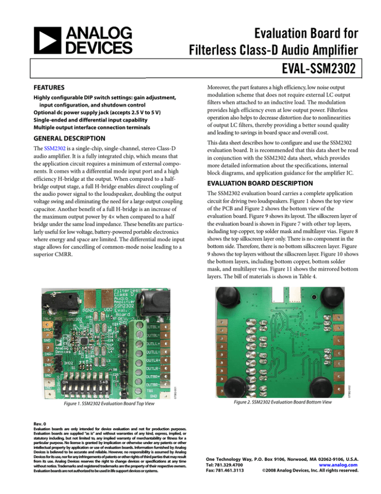
The SSM2302 evaluation board carries a complete application
circuit for driving two loudspeakers. Figure 1 shows the top view
of the PCB and Figure 2 shows the bottom view of the
evaluation board. Figure 9 shows its layout. The silkscreen layer of
the evaluation board is shown in Figure 7 with other top layers,
including top copper, top solder mask and multilayer vias. Figure 8
shows the top silkscreen layer only. There is no component in the
bottom side. Therefore, there is no bottom silkscreen layer. Figure
9 shows the top layers without the silkscreen layer. Figure 10 shows
the bottom layers, including bottom copper, bottom solder
mask, and multilayer vias. Figure 11 shows the mirrored bottom
layers. The bill of materials is shown in Table 4.
07582-001
The SSM2302 is a single-chip, single-channel, stereo Class-D
audio amplifier. It is a fully integrated chip, which means that
the application circuit requires a minimum of external components. It comes with a differential mode input port and a high
efficiency H-bridge at the output. When compared to a halfbridge output stage, a full H-bridge enables direct coupling of
the audio power signal to the loudspeaker, doubling the output
voltage swing and eliminating the need for a large output coupling
capacitor. Another benefit of a full H-bridge is an increase of
the maximum output power by 4× when compared to a half
bridge under the same load impedance. These benefits are particularly useful for low voltage, battery-powered portable electronics
where energy and space are limited. The differential mode input
stage allows for cancelling of common-mode noise leading to a
superior CMRR.
Moreover, the part features a high efficiency, low noise output
modulation scheme that does not require external LC output
filters when attached to an inductive load. The modulation
provides high efficiency even at low output power. Filterless
operation also helps to decrease distortion due to nonlinearities
of output LC filters, thereby providing a better sound quality
and leading to savings in board space and overall cost.
07582-002
FEATURES
Figure 1. SSM2302 Evaluation Board Top View
Figure 2. SSM2302 Evaluation Board Bottom View
Evaluation boards are only intended for device evaluation and not for production purposes.
Evaluation boards are supplied “as is” and without warranties of any kind, express, implied, or
statutory including, but not limited to, any implied warranty of merchantability or fitness for a
particular purpose. No license is granted by implication or otherwise under any patents or other
intellectual property by application or use of evaluation boards. Information furnished by Analog
Devices is believed to be accurate and reliable. However, no responsibility is assumed by Analog
Devices for its use, nor for any infringements of patents or other rights of third parties that may result
from its use. Analog Devices reserves the right to change devices or specifications at any time
without notice. Trademarks and registered trademarks are the property of their respective owners.
Evaluation boards are not authorized to be used in life support devices or systems.
One Technology Way, P.O. Box 9106, Norwood, MA 02062-9106, U.S.A.
www.analog.com
Tel: 781.329.4700
Fax: 781.461.3113
©2008 Analog Devices, Inc. All rights reserved.
Rev. 0
EVAL-SSM2302
TABLE OF CONTENTS
Features .............................................................................................. 1 Component Selections ..................................................................4 General Description ......................................................................... 1 Layout Guidelines..........................................................................5 Evaluation Board Description......................................................... 1 Evaluation Board Schematic and Artwork.....................................6 Revision History ............................................................................... 2 Ordering Information .......................................................................8 Evaluation Board Hardware ............................................................ 3 Bill of Materials ..............................................................................8 Switches.......................................................................................... 3 Ordering Guide .............................................................................8 Getting Started .............................................................................. 3 ESD Caution...................................................................................8 What to Test .................................................................................. 4 REVISION HISTORY
8/08—Revision 0: Initial Version
Rev. 0 | Page 2 of 8
EVAL-SSM2302
EVALUATION BOARD HARDWARE
Note that the SSM2302 evaluation board and layout guidelines
were developed by Gang Liu of Analog Technologies, Inc.,
Sunnyvale, CA.
SWITCHES
On the upper left corner of the evaluation board is an audio
stereo jack connector (3.5 mm), J1. It accepts standard stereo
audio signals by using a conventional audio stereo signal connector/cable to receive audio signals from common appliances
such as DVD players, personal computers, and TVs. Note that
the two output signals from the J1 connector are combined by
a resistor network, R1 and R2, into a single signal. When this
input connector is utilized, turn the switches, S1E and S1F, to
the upper positions, to ac short circuit the negative input ports to
ground; this connector only provides single-ended audio signals.
This signal path is shown in the schematic in Figure 6. Some
appliances may have strong ground noise. In the event that the
audio source has strong ground noise, do not use the J1 connector
as the input connection point. A single-ended input signal with
strong ground noise generates an audible hissing sound at the
output. When this happens, differential mode connection is
needed and the ground noise interference can be cancelled.
The switches, S1E and S1F, as briefly described previously, are
used to ac short circuit the left and right channel negative input
ports, respectively, to ground. This function is generally recommended, but only necessary when driving the input ports in
single-ended mode. After shorting the negative input ports to
ground, the noise picked up by the input port connections is
conducted to the ground.
S1G controls the gain. Place S1G in the upper position for the
higher gain and place it in the lower position for the lower gain.
S1H is for the shutdown function. The upper position is for
shutdown and the lower position turns the amplifier on.
The upper right corner has a dc power jack connector. The
center pin is for the positive terminal, which accepts 3 V to 5 V.
When the input voltage is 5 V, the maximum peak current is
approximately 0.6 A when driving an 8 Ω load.
There are two solder pads in the upper center edge area for
connecting the power supply voltages by clipping or soldering.
All the output ports are located on the right side of the board
and marked properly with labels. See the legend on the evaluation
board in Figure 1 and the schematic in Figure 6.
When differential mode audio signals are used as the input
signal source, use either the 3HD1 and 3HD2 headers or the
soldering pads located on the left side of the board. The top
header is for the left channel signals and the bottom header is
for the right channel. At the same time, turn the S1E and S1F
switches to their off positions (the lower position).
There are three ways to connect the output signals to the loads
(the loudspeakers): using the four 2-pin headers, the terminal
block, or the soldering pads.
There are two ground soldering pads on the lower left corner.
1.
GETTING STARTED
To ensure proper operation, follow these steps carefully:
•
On the lower side of the board is a switch bank; the
corresponding channels are shown in Table 1.
•
Table 1. Switch Pin Nomenclature
Switch Name
S1A
S1B
S1C
S1D
S1E
S1F
S1G
S1H
Verify that the control switches are at the proper positions.
Corresponding Channel
AC couple left channel noninverting input
AC couple left channel inverting input
AC couple right channel inverting input
AC couple right channel noninverting input
AC ground left channel inverting input
AC ground right channel inverting input
Gain control pin
Shutdown
When the S1A, S1B, S1C, and S1D switches are placed in the up
position, their corresponding coupling capacitors are shorted;
when these switches are placed in the down position, the coupling
capacitors are inserted in the signal paths.
•
•
2.
3.
Rev. 0 | Page 3 of 8
Shutdown control: S1H down. This activates the
amplifier.
Gain setting: S1G. Select the position based on the
gain needed.
Audio source: S1E and S1F. For single-ended mode
(audio jack), put S1E and S1F in the upper position.
Input coupling: S1A, S1B, S1C, and S1D. For most
applications, ac couple the inputs by setting these
switches in the lower position.
Connect the loads to the proper output ports. Depending
on the application, different nodes should be used. To
connect the loads right after the beads, use the OUTBL+,
OUTBL−, OUTBR+, and OUTBR− nodes. To connect the
loads after the inductors, use the OUTLL+, OUTLL−,
OUTLR+, and OUTLR− nodes.
Connect the power supply with the correct polarity and
proper voltage.
EVAL-SSM2302
WHAT TO TEST
Output Beads—B1, B2, B3, and B4
The EVAL-SSM2302 tests the following:
B1, B2, B3, and B4 are necessary components for filtering out the
EMIs caused at the switching output nodes. Make sure that these
beads have enough current conducting capability while providing
sufficient EMI attenuation. The current rating needed for an 8 Ω
load is about 600 mA, and the impedance at 100 MHz must be
≥220 Ω. In addition, the lower the dc resistance (DCR) of these
beads, the better for minimizing their power consumptions.
The recommended bead is detailed in Table 2.
•
•
•
•
•
•
Electromagnetic interference (EMI). Connect wires for the
speakers in the same length as for the actual application
situation and complete the EMI test.
Signal-to-noise ratio.
Total harmonic distortion (THD).
Output noise. Make sure to use an A-weighted filter to
filter the output before the measurement meter.
Maximum output power.
Efficiency.
Output Shunting Capacitors for the Beads
There are two groups of output shunting capacitors. C11, C12,
C13, and C14 are for filtering out the lower frequency EMIs of
up to 250 MHz. C23, C24, C25, and C26 are for filtering out the
higher frequency EMIs of >250 MHz. Use small size (0603 or
0402) multilayer ceramic capacitors that are made of X7R or
COG (NPO) materials. The higher the value of these capacitors,
the lower the residual EMI level at the output, and the higher the
quiescent current at the power supply. Using 500 pF to 1 nF values
for the first group of capacitors and using 100 pF to 200 pF for
the second group of capacitors is recommended.
COMPONENT SELECTIONS
Selecting the right components is the key to achieving the performance required at the cost budgeted. The bill of materials for
the SSM2302 evaluation board is shown in Table 4.
Input Coupling Capacitor Selection—C1, C2, C3, and C4
The capacitors, C1, C2, C3, and C4, should be large enough to
couple the low frequency signal components in the incoming
signal and small enough to filter out unnecessary low frequency
signals. For music signals, the cutoff frequency is often chosen
between 20 Hz and 50 Hz. The value of the input capacitor is
calculated by
Output Inductors
Some users do not want high frequency EMIs in their systems
and prefer to use inductors to filter out the high frequency
components at the output node. Select inductance >2.2 μH for
these inductors. The higher the inductance, the lower the EMI
at the output, and the lower the quiescent current at the power
supply, but the higher the power consumption by the inductors
when the output power level is high. Using 2.2 μH to 10 μH
inductors is recommended and the current rating needs >600 mA
(saturation current) for an 8 Ω load. Table 3 shows the recommended inductors. Note that these inductors are not populated
on the evaluation board.
C = 1/(2πRfc)
where:
R = 150 kΩ + REXT.
fc is the cutoff frequency.
Input Serial Resistors—R1, R2, R3, and R4
R1, R2, R3, and R4 are not necessary for amplifier operation and
are only needed when special gain values are required. To
determine the proper gain value, use the following formula:
External Gain Settings = 20 log [2/(1 + R/150 kΩ)]
Warning
Using large value resistors can increase the input noise.
Table 2. Recommended Output Bead
Part No.
BLM18EG221SN1
Manufacturer
Murata
Z (Ω)
220
IMAX (mA)
2000
DCR (Ω)
0.05
Size (mm)
1.6 × 0.8 × 0.8
L (μH)
4.7
3.3
2.2
10
10
2.2
4.7
IMAX (mA)
650
710
790
900
690
630
680
DCR (Ω)
0.15
0.12
0.1
0.3
0.18
0.13
0.31
Size (mm)
3.2 × 2.5 × 1.55
3.2 × 2.5 × 1.55
3.2 × 2.5 × 1.55
3.1 × 3.1 × 1.8
3.8 × 3.8 × 1.8
2.5 × 1.8 × 2
3.8 × 3.8 × 1
Table 3. Recommended Output Inductors
Part No.
LQH32CN4R7M53
LQH32CN3R3M53
LQH32CN2R2M53
SD3118-100-R
ELL4LM100M
LBC2518T2R2M
1033AS-4R7M
Manufacturer
Murata
Murata
Murata
Cooper Bussmann
Panasonic
Taiyo Yuden
Toko
Rev. 0 | Page 4 of 8
EVAL-SSM2302
LAYOUT GUIDELINES
To keep the EMI under the allowable limit and to ensure that
the amplifier chip operates under the temperature limit, PCB
layout is critical in application designs. Follow these guidelines
carefully when setting up the PCB layout designs.
9.
10.
1.
11.
5.
6.
7.
8.
The SSM2302 works well only if these techniques are implemented
in the PCB design to keep EMI and the amplifier temperature low.
TOP LAYER
INTERNAL AND/
OR BOTTOM
LAYER
Figure 3. Heat Sink Layout
COPPER
FILL
B1
B2
C12
C11
C24
C23
C19
C25
C26
SMALL
INDUCTOR
B4
B3
C13
OUTPUT
TRACK
C14
INPUT
TRACK
07582-004
4.
13.
Figure 4. Placement and Routing for the Decoupling Capacitors
COPPER
FILL
B1
B2
C12
C11
C24
C23
C19
C25
C26
B4
SMALL
INDUCTOR
B3
C13
C14
INPUT
TRACK
OUTPUT
TRACK
07582-005
3.
12.
07582-003
2.
Place nine vias onto the thermal pad of the amplifier. The
outer diameter of the vias should be 0.5 mm and the inner
diameter is 0.33 mm. If there are internal layers available in
the PCB, allocate an area as large as possible as the ground
planes and let these vias be connected to the planes (see
Figure 3). If internal layers are available, allocate a certain
area as a heat sink, and make sure to connect the vias
conducting the heat to the internal layers.
Place the EMI filtering beads, B1, B2, B3, B4, and B5, as
close to the amplifier chip as possible. The same principle
applies to the output inductors, L1, L2, L3, and L4, if they
exist in the application design.
Place the decoupling capacitors for the beads, C11, C12,
C13, C14, C23, C24, C25, and C26, as close to the amplifier
chip as possible, and connect all their ground terminals
together as close as possible, as shown in Figure 4. The
same principle applies to the decoupling capacitors for the
inductors, C15, C16, C17, and C18, if they exist in the
application design. Ideally, solder their ground terminals
together; do not rely on PCB tracks or ground planes for
connecting their ground terminals together.
Place the decoupling capacitor for the power supply, C19,
as close to the amplifier chip as possible, as shown in
Figure 4, and connect its ground terminal directly to the IC
ground pins, Pin 13 and Pin 16.
Place the decoupling capacitor for the power supply, C20,
as close to the amplifier chip as possible, and connect the
ground terminal to the PCB ground plane where it shares a
common ground with the power supply.
Place the bead for the power supply, B5, as close to the
amplifier chip as possible, and keep it on the same side of
the PCB where the chip stays.
The 1 nF capacitor and the ferrite bead can block the EMI for
up to 250 MHz. To eliminate EMIs higher than the 250 MHz,
place a low value small size capacitor, such as 100 pF 0402
size, in parallel with the decoupling capacitors, C11, C12,
C13, and C14. However, place this small capacitor a short
distance away, at least 20 mm, from the 1 nF decoupling
capacitor. Ideally, the ground terminals of these capacitors
are connected to the ground terminals or the PCB traces,
which are placed as close to the output loads (loudspeakers)
as possible. In this way, the PCB connecting trace between
these two capacitors serves as an inductor for filtering out
the high frequency component, as shown in Figure 4.
Decouple the input port nodes and the digital pins, Pin 3,
Pin 4, Pin 5, Pin 8, Pin 9, and Pin 10, with small capacitors,
such as 100 pF. The capacitors are not necessary, but can
lower the EMI from these pins. The ground terminals of
these capacitors should be connected to the chip ground as
close as possible. See Figure 7, Figure 8, and Figure 9.
Ground the unconnected pins, Pin 6 and Pin 7.
Connect the ground pins, Pin 6, Pin 7, Pin 13, and Pin 16,
to the thermal pad and place grounding vias, as shown in
Figure 7, Figure 8, and Figure 9.
Use a solid polygon plane on the other side of the PCB for
the area of the vias, which are placed on the thermal pad of
the chip (see Figure 10 and Figure 11). This polygon serves
as both the EMI shielding ground plane and the heat sink
for the SSM2302.
Keep the PCB traces of high EMI nodes on the same side of
the PCB and as short as possible. Pin 1, Pin 2, Pin 11, and
Pin 12 are the high EMI nodes.
The incoming and outgoing PCB tracks to the output
decoupling capacitors should not be connected to each
other. The correct layout is shown in Figure 4. An example
of an incorrect layout is shown in Figure 5.
Figure 5. Incorrect Routing for the Output Decoupling Capacitor
Rev. 0 | Page 5 of 8
3HD1
3
2
1
1
1
GND
INR -
INR+
1
1
1
3P_HEADER
3HD2
3
2
1
2
3
1
SJ-3523A
J1
3P_HEADER
GND
INL -
4
3
2
1
C1
2
2
2
1
2
8PST
22nF
S1D
C4
8PST
S1C
22nF
1
C3
8PST
S1B
22nF
1
C2
8PST
S1A
22nF
1
2
13
14
15
16
1
C5
100pF
2
1
2
1
2
1
12
5
8PST
S1E
C9
22nF
R5
20
C6
100pF
2
1
2
1
2
1
11
6
INL+
100
R3
100
R2
100
R1
8PST
S1F
C10
22nF
R6
20
1
1
1
C7
100pF
2
2
2
8
8
7
6
5
2
1nF
C21
1
100pF
C8
INR-
NC
NC
INL-
8PST
S1H
1
2
4
3
U1
SSM2302
R4
100
9
INL+
INR+
9
GAIN
10
10
7
2
1
SD
2
OUTLOUTR-
1
1
B1
2
1
13
14
15
16
B3
GND
VDD
VDD
GND
PAD
2
1
2
100K
R8
C22
1nF
2
1
BLM18EG221SN1
B4
VDD
BLM18EG221SN1
BLM18EG221SN1
2 R7
1
VDD
100K
B2
1
2
BLM18EG221SN1
S1G
8PST
11
OUTL+
OUTR+
1
100pF
100pF
C19
10uF
BLM18EG221SN1
1
2
C15
L1
3.3uH
(NO_POP)
C17
1uF
L3
3.3uH
(NO_POP)
1uF
VDD
C20
10uF
100pF
C26
B5
C25
1nF
1nF
C13
C14
1nF
C23
1nF
100pF
C12
C24
C11
2
12
2
1
2
1
2
1
1
2
2
1
2
1
1
1
1
2
1
2
2
2
1
2
1
2
1
2
2
1
1
2
1
2
1
1
2
2
Rev. 0 | Page 6 of 8
1
Figure 6. Schematic of SSM2302 Evaluation Board
L4
3.3uH
(NO_POP)
1uF
C18
1uF
C16
L2
3.3uH
(NO_POP)
3
2
1
1
1
2
1
2
1
2
1
2
1
2
1
PGND
VDD
J2
PS_JACK
2PINA
2HD5
2PINA
2HD4
2PINA
2HD3
2PINA
2HD2
2PINA
2HD1
TB1
OUTLL -
OUTLL+
OUTBL-
1
1
1
1
1
1
GND
GND
OUTBR-
OUTBR+
OUTLR-
OUTLR+
10P_T_BLOCK
10
9
8
7
6
5
4
3
2
1
1
1
1
OUTBL+
07582-006
1
EVAL-SSM2302
EVALUATION BOARD SCHEMATIC AND ARTWORK
07582-010
07582-007
EVAL-SSM2302
Figure 10. Bottom Layers
Figure 11. Mirrored Bottom Layers
07582-009
Figure 8. Top Silkscreen
07582-011
07582-008
Figure 7. Top Silkscreen Layer with Other Top Layers
Figure 9. Top Layers Without Top Silkscreen Layer
Rev. 0 | Page 7 of 8
EVAL-SSM2302
ORDERING INFORMATION
BILL OF MATERIALS
Table 4.
Qty.
4
2
2
6
8
6
4
2
4
5
1
1
1
1
5
2
1
Designator
R1, R2, R3, R4
R5, R6
R7, R8
C1, C2, C3, C4, C9,
C10
C5, C6, C7, C8, C23,
C24, C25, C26
C11, C12, C13, C14,
C21, C22
C15, C16, C17, C18
C19, C20
L1, L2, L3, L4
B1, B2, B3, B4, B5
S1
J1
J2
U1
2HD1, 2HD2, 2HD3,
2HD4, 2HD5
3HD1, 3HD2
TB1
Description
Resistor, 100 Ω, 1/16 W, 0.5%, 0402 SMD
Resistor, 20 Ω, 1/16 W, 0.5%, 0402 SMD
Resistor, 100 kΩ, 1/16 W, 0.5%, 0402 SMD
Capacitor, ceramic, 22 nF, 50 V, X7R 0402
Supplier
Digi-Key
Digi-Key
Digi-Key
Digi-Key
Supplier Part No.
RR05P100DTR-ND
RR05R20DTR-ND
RR05P100DTR-ND
490-3884-2-ND
Capacitor, ceramic, 100 pF, 6.3 V, X7R 0402
Digi-Key
04026C101KAT2A-ND
Capacitor ceramic, 1 nF, 5%, 50 V, X7R 0402
Digi-Key
478-3661-2-ND
Capacitor, ceramic, 1 μF, 10 V, X5R 0402
Capacitor, ceramic, 10 μF, 6.3 V, X5R 0603
Inductor, 3.3 μH, 710 mA, 0.12 Ω DCR, 3.2 × 2.5 × 1.55
Filter chip, 220 Ω, 2 A, 0603
Switch DIP top slide, 8-position, SMD, SDA08H1SBDA
Audio connectors, 3.5 mm, SMT, stereo, black, 3-position, all
plastic, SJ-3523A
DC power connector, 2 mm, SMT power jack
Filterless, high efficiency, Class-D, stereo audio amplifier
Connector header, 2-position, 0.100 inch SGL gold
Digi-Key
Digi-Key
Murata
Digi-Key
Digi-Key
Mouser
490-3890-2-ND
PCC2395TR-ND
LQH32CN3R3M53
490-3992-2-ND
CKN6092-ND
806-STX-3500-3N
Mouser
Analog Devices
Digi-Key
806-KLDX-SMT2-0202-A
SSM2302CPZ
SAM1029-02-ND
Connector header, 3-position, 0.100 inch SGL gold
Terminal block, 3.5 mm, 10-position PCB
Digi-Key
Digi-Key
SAM1029-03-ND
ED1522-ND
ORDERING GUIDE
Model
SSM2302Z-EVAL1
1
Description
Evaluation Board
ESD CAUTION
Z = RoHS Compliant Part.
©2008 Analog Devices, Inc. All rights reserved. Trademarks and
registered trademarks are the property of their respective owners.
EB07582-0-8/08(0)
Rev. 0 | Page 8 of 8


