D ATA S H E E T
Features
OPTAN BALL LENS—UVC LEDS IN A TO-39 PACKAGE WHICH
> FOCUSED RADIATION PATTERN WITH A VIEWING ANGLE OF 15°
OFFERS SUPERIOR LIGHT OUTPUT, EXCELLENT SPECTRAL
> PEAK WAVELENGTHS FROM 250 nm - 280 nm
> AVAILABLE IN LIGHT OUTPUT BINS FROM 0.5 mW TO > 3 mW
QUALITY AND LONG LIFETIMES. AVAILABLE IN PEAK
> MAXIMUM DRIVE CURRENT OF 100 mA IN CONTINUOUS MODE
WAVELENGTHS FROM 250 nm-280 nm AND OPTICAL OUTPUT
> TYPICAL L50 LIFETIME OF 3000 HOURS AT 100 mA
> HERMETIC, THROUGH-HOLE PACKAGE
BINS FROM 0.5 mW TO > 3 mW, THESE LEDS ARE IDEAL FOR
> RoHS COMPLAINT
SPECTROSCOPIC APPLICATIONS IN ANALYTICAL AND LIFE
Benefits
SCIENCES INSTRUMENTATION.
> BUILT-IN LENS PROVIDES LIGHT FOCUS, AND REDUCES ASSEMBLY COST
> NARROW SPECTRUM ENABLES ELIMINATION OF FILTERS
> RELATIVELY LOW SYSTEM COST
> SUPERIOR IRRADIANCE (mW/nm/cm2)
> ENVIRONMENT ISOLATED PACKAGE
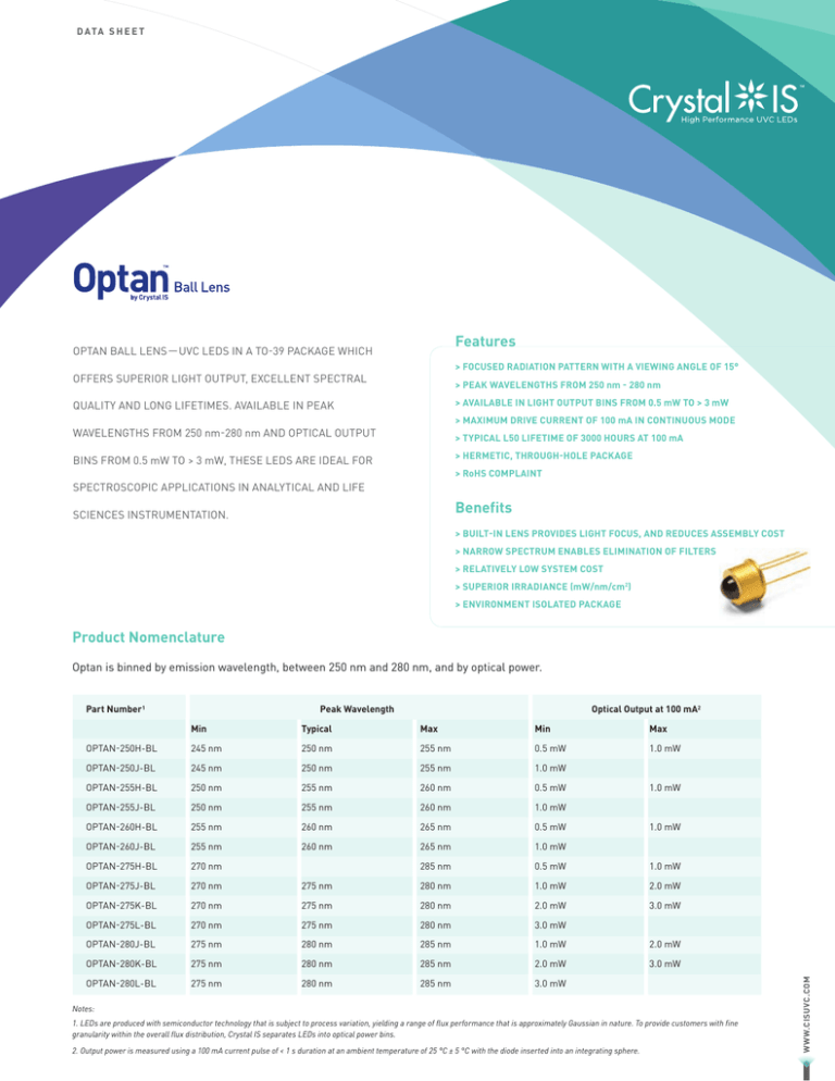
Product Nomenclature
Optan is binned by emission wavelength, between 250 nm and 280 nm, and by optical power.
Peak Wavelength
Optical Output at 100 mA2
Min
Typical
Max
Min
Max
OPTAN-250H-BL
245 nm
250 nm
255 nm
0.5 mW
1.0 mW
OPTAN-250J-BL
245 nm
250 nm
255 nm
1.0 mW
OPTAN-255H-BL
250 nm
255 nm
260 nm
0.5 mW
OPTAN-255J-BL
250 nm
255 nm
260 nm
1.0 mW
OPTAN-260H-BL
255 nm
260 nm
265 nm
0.5 mW
OPTAN-260J-BL
255 nm
260 nm
265 nm
1.0 mW
OPTAN-275H-BL
270 nm
285 nm
0.5 mW
1.0 mW
OPTAN-275J-BL
270 nm
275 nm
280 nm
1.0 mW
2.0 mW
OPTAN-275K-BL
270 nm
275 nm
280 nm
2.0 mW
3.0 mW
OPTAN-275L-BL
270 nm
275 nm
280 nm
3.0 mW
OPTAN-280J-BL
275 nm
280 nm
285 nm
1.0 mW
2.0 mW
OPTAN-280K-BL
275 nm
280 nm
285 nm
2.0 mW
3.0 mW
OPTAN-280L-BL
275 nm
280 nm
285 nm
3.0 mW
1.0 mW
1.0 mW
Notes:
1. LEDs are produced with semiconductor technology that is subject to process variation, yielding a range of flux performance that is approximately Gaussian in nature. To provide customers with fine
granularity within the overall flux distribution, Crystal IS separates LEDs into optical power bins.
2. Output power is measured using a 100 mA current pulse of < 1 s duration at an ambient temperature of 25 °C ± 5 °C with the diode inserted into an integrating sphere.
WWW.CISUVC.COM
Part Number1
D ATA S H E E T : O P TA N B A L L L E N S
LED Characteristics1
Characteristic
Unit
Viewing angle
degrees
15
Full width at half maximum
nm
11
Forward voltage at 100 mA
V
Lifetime, L50 at 100 mA
hours
3000
Lifetime, L50, at 20 mA4
hours
8000
Thermal resistance, junction-to-case
°C/W
20
Power dissipation at 100 mA
W
2
3
4
Min.
Typical
Max.
10
1.0
Notes:
1. All measurements completed at an ambient temperature of 25 °C wherever applicable.
2. Viewing angle is twice of half-value angle. A half-value angle is the angle between axial direction and direction in which the light intensity value is half of the axial intensity.
3. Voltage tolerance is ±5 %.
4. L50 is the time at which light output drops to 50 % of original value during continuous operation at 25 °C.
Absolute Maximum Ratings
Characteristic
Unit
Min.
Forward current (continuous or CW)
mA
Reverse voltage
V
Operating temperature range
°C
-5
Storage temperature
°C
-40
Junction temperature
°C
Typical
Max.
100
-5
55
100
85
Typical Radiation Pattern
Typical Electrical Characteristics
Optan LEDs with a ball lens have a nominal viewing angle
of 15°.
The typical forward voltage is less than 10 V at an operating
current of 100 mA.
R A D I AT I O N PAT T E R N
T Y P I CA L E L E CT R I CA L C H A R ACT E R I S T I C S
100
90
75
80
60
0.8
135
0.6
150
45
30
60
40
0.4
165
15
20
0.2
0.0
180
0
0
0
1
2
3
4
5
6
7
8
9
10
VOLTAGE, V
Test Conditions: I (CW) = 100 mA, CW = Continuous Wave Mode
Test Conditions: I (Pulsed mode) = 1 to 100 mA; Case Temperature (TC ) = 25 °C
WWW.CISUVC.COM
NORMALIZED INENSITY, a.u.
120
CURRENT, mA
105
1.0
D ATA S H E E T : O P TA N B A L L L E N S
Typical Spectral Characteristics Over Current
Typical Light Output Characteristics Over Current
The plot below shows the stability of the peak wavelength with
various applied currents. No shift is typically observed in the peak
wavelength with change in drive current from 100 mA to 20 mA.
The plot below shows the typical variation in light output with
forward current. The light output data is normalized to the light
output at 100 mA.
S P E CT R U M V S . C U R R E N T
L I G H T O U T P U T OV E R C U R R E N T
100
1.0
INTENSTIY, a.u.
RELATIVE LIGHT OUTPUT, %
100 mA
60 mA
20 mA
0.8
0.6
0.4
0.2
80
60
40
20
0
0.0
-20
-10
0
10
0
20
20
40
60
80
100
FORWARD CURRENT (PULSE), mA
WAVELENGTH OFFSET FROM PEAK, nm
Test Conditions: Case Temperature (TC ) = 25 °C
Test Conditions: Case Temperature (TC ) = 25 °C
Typical Spectral Characteristics Over
Temperature
Typical Light Output Characteristics Over
Temperature
The plot below illustrates the stability of the spectral
characteristics with change in temperature. No shift is
typically observed in the peak wavelength with change in
case temperature from 20 °C to 60 °C.
Output power is very sensitive to junction temperature, so
proper thermal management techniques are suggested to
control junction temperature. Lower junction temperatures
will ensure the optimal performance and lifetime of the LED.
The plot below shows the change in optical power with increase
in junction temperature. A typical drop of 5 % in light output is
noticed for a 10 °C rise in temperature.
S P E CT R U M V S . T E M P E R AT U R E
L I G H T O U T P U T OV E R T E M P E R AT U R E
1.0
20 ºC
40 ºC
60 ºC
0.8
INTENSTIY, a.u.
RELATIVE LIGHT OUTPUT, %
100
0.6
0.4
0.2
90
80
70
60
20
-20
-10
0
10
20
30
40
50
WAVELENGTH OFFSET FROM PEAK, nm
Test Conditions: I (Pulsed Mode) = 100 mA
60
70
80
90
J U N C T I O N T E M P E R A T U R E ( TJ) , º C
Test Conditions: I (Pulsed Mode) = 100 mA
WWW.CISUVC.COM
0.0
D ATA S H E E T : O P TA N B A L L L E N S
Recommended Operation
C U R R E N T D E R AT I N G C U R V E
120
ALLOWABLE FORWARD CURRENT, mA
Crystal IS LEDs should be operated at currents below 100 mA
and mounted on a heat sink to keep the case temperature
below 55 °C. Please refer to the Crystal IS thermal management
note AN003 for heat sink recommendations. Circuits should
be designed for constant current.
100
80
60
40
20
0
-10
0
10
20
30
40
50
60
C A S E T E M P E R AT U R E ( T C) , º C
Test Conditions: CW
Mechanical Dimensions
The Optan package is comprised of a header with a copper slug and a Kovar cap that is welded to the header to provide hermetic
sealing. The cap contains a fused silica ball lens which provides the nominal viewing angle of 15°.
O P TA N TO - 3 9 PA C K A G E W I T H B A L L L E N S
Ø 5.4 ±0.005
Ø 9.15
Ø 8.4
cathode
5.8 nom.
2.4
anode
+0.05
-0.07
case
0
+0.050
-0.025
R2.54
°
45
°
Ø 0.43
45
13.46 ± 0.75
Ø 3.5 -0.01
WWW.CISUVC.COM
All dimensions are in millimeters. Unless noted otherwise, all dimensions have a tolerance of ± 0.05 mm.
D ATA S H E E T : O P TA N B A L L L E N S
Recommended Soldering Guidelines
1. The pitch of the LED lead should match the pitch of the mounting holes on the PCB during component placement.
2. The tip of the soldering iron should never touch the lens.
3. Recommended soldering pattern is illustrated in Figure 1. In addition, please ensure that the central copper slug in the
header is thermally connected to the board with thermal paste or grease. A heat sink should be used to keep the case
temperature of the LED below 55 °C at aforward current of 100 mA. Please refer to the Crystal IS thermal management
note AN003 for heat sink recommendations.
4. After soldering, avoid applying external force, stress, and excessive vibration until the product has returned to
ambient temperature.
Recommended Soldering Conditions
Distance between melted solder sides to bottom of LED should be 3 mm or longer.
Parameter
Dip Soldering (Lead Free Solder)
Pre Heat
90 °C max. (Backside of PCB)
Hand Soldering (Lead Free Solder)
--
Pre Heat Time
60 seconds max.
--
Temperature
260 °C max. (Solder Bath)
300 °C max. (Soldering Iron Tip)
Soldering Time
5 seconds max.
3 seconds max.
Recommended Cleaning
> Cleaning
with isopropyl alcohol is recommended. Propanol and ethyl alcohol may also be used.
> DO
NOT use ultrasonic cleaners with Crystal IS LEDs.
> DO
NOT use acetone or trichloroethylene to clean Crystal IS LEDs.
Problems with LEDs such as reduction in light output, opens, or shorts can be prevented as long as the LEDs are
soldered under these conditions.
CIRCUIT BOARD
Figure 1
COPPER SLUG (TOP)
THERMAL PAD (BOTTOM)
WWW.CISUVC.COM
THERMAL PASTE (MIDDLE)
Eye Safety Guidelines
During operation, the LED emits high intensity ultraviolet (UV)
light, which is harmful to skin and eyes. UV light is hazardous to
skin and may cause cancer. Avoid exposure to UV light when LED
is operational. Precautions must be taken to avoid looking directly
at the UV light without the use of UV light protective glasses. Do
not look directly at the front of the LED or at the LED’s lens when
LED is operational.
Disclaimer
Attach the following warning labels on
products/systems that use UV LEDs.
RoHS Compliance
The levels of environmentally sensitive, persistent biologically
toxic (PBT), persistent organic pollutants (POP), or otherwise
restricted materials in this product are below the maximum
concentration values (also referred to as the threshold limits)
permitted for such substances, or are used in an exempted
application, in accordance with EU Directive 2002/95/EC on
the restriction of the use of certain
hazardous substances in electrical
and electronic equipment (RoHS),
as amended through April 21, 2006.
Handling Precautions
LEDs are sensitive to static electricity. When handling, proper ESD
protection is required, including:
> Eliminating
static charge
> Using
grounded wriststrap, ESD footwear,
clothes, and floors
> Grounded
workstation and tools.
We invite you to learn more about our UVC LEDs.
70 Cohoes Avenue
Green Island, NY 12183
U.S.A.
www.cisuvc.com
518.271.7375
sales@cisuvc.com
©2015 Crystal IS, Inc. All rights reserved. Crystal IS and the Crystal IS logo are trademarks of Crystal IS, Inc.
and/or its affiliates. All other trademarks are the property of their respective owners. 1004-1509
The information in this document has
been compiled from reference materials
and other sources believed to be reliable,
and given in good faith. No warranty, either
expressed or implied, is made, however,
to the accuracy and completeness of the
information, nor is any responsibility
assumed or implied for any loss or damage
resulting from inaccuracies or omissions.
Each user bears full responsibility for
making their own determination as to
the suitability of Crystal IS products,
recommendations or advice for its own
particular use. Crystal IS makes no
warranty or guarantee, express or implied,
as to results obtained in end-use, nor of
any design incorporating its Products,
recommendation or advice.
Each user must identify and perform
all tests and analyses necessary to
ensure that it’s finished application
incorporating Crystal IS’ products will
be safe and suitable for use under end-use
conditions. Each user of devices assumes
full responsibility to become educated in
and to protect from harmful irradiation.
Crystal IS specifically disclaims any and
all liability for harm arising from buyer’s
use or misuse of UVC devices either in
development or end-use.
