MP1541
1.3MHz Boost Converter
The Future of Analog IC Technology
DESCRIPTION
FEATURES
The MP1541 is a 5-pin thin SOT23 current
mode step up converter intended for small, low
power applications. The MP1541 switches at
1.3MHz and allows the use of tiny, low cost
capacitors and inductors 2mm or less in height.
Internal soft start results in small inrush current
and extends battery life. The MP1541 operates
from an input voltage as low as 2.5V and can
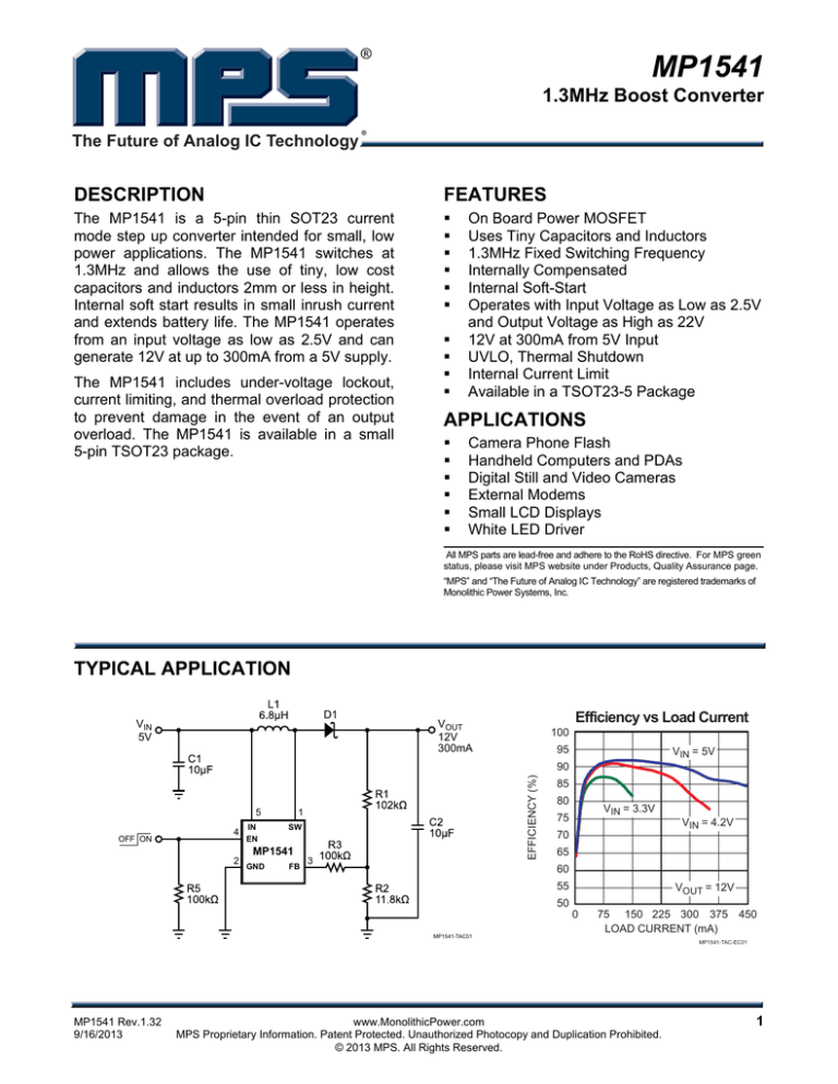
generate 12V at up to 300mA from a 5V supply.
The MP1541 includes under-voltage lockout,
current limiting, and thermal overload protection
to prevent damage in the event of an output
overload. The MP1541 is available in a small
5-pin TSOT23 package.
On Board Power MOSFET
Uses Tiny Capacitors and Inductors
1.3MHz Fixed Switching Frequency
Internally Compensated
Internal Soft-Start
Operates with Input Voltage as Low as 2.5V
and Output Voltage as High as 22V
12V at 300mA from 5V Input
UVLO, Thermal Shutdown
Internal Current Limit
Available in a TSOT23-5 Package
APPLICATIONS
Camera Phone Flash
Handheld Computers and PDAs
Digital Still and Video Cameras
External Modems
Small LCD Displays
White LED Driver
All MPS parts are lead-free and adhere to the RoHS directive. For MPS green
status, please visit MPS website under Products, Quality Assurance page.
“MPS” and “The Future of Analog IC Technology” are registered trademarks of
Monolithic Power Systems, Inc.
TYPICAL APPLICATION
D1
VIN
5V
Efficiency vs Load Current
VOUT
12V
300mA
100
95
VIN = 5V
5
OFF ON
IN
4
EN
2
1
SW
MP1541
GND
EFFICIENCY (%)
90
FB
3
85
80
VIN = 3.3V
75
70
VIN = 4.2V
65
60
55
50
MP1541-TAC01
VOUT = 12V
0
75 150 225 300 375 450
LOAD CURRENT (mA)
MP1541-TAC-EC01
MP1541 Rev.1.32
9/16/2013
www.MonolithicPower.com
MPS Proprietary Information. Patent Protected. Unauthorized Photocopy and Duplication Prohibited.
© 2013 MPS. All Rights Reserved.
1
MP1541 – 1.3MHz BOOST CONVERTER
ORDERING INFORMATION
Part Number*
MP1541DJ
Package
TSOT23-5
Top Marking
B3
Free Air Temperature (TA)
–40°C to +85°C
* For Tape & Reel, add suffix –Z (e.g. MP1541DJ–Z)
For RoHS compliant packaging, add suffix –LF (e.g. MP1541DJ–LF–Z)
PACKAGE REFERENCE
TOP VIEW
1
GND
2
FB
3
5
IN
4
EN
B3YW
SW
MP1541-PD01-TSOT23
ABSOLUTE MAXIMUM RATINGS (1)
SW Pin ...........................................–0.3V to 25V
All Other Pins ................................–0.3V to 6.5V
Junction Temperature ...............................150°C
(2)
Continuous Power Dissipation (TA = +25°C)
........................................................... 0.47W
Lead Temperature ....................................260°C
Storage Temperature.............. –65°C to +150°C
Recommended Operating Conditions
(3)
Supply Voltage VIN .............................2.5V to 6V
Output Voltage VOUT ............................3V to 22V
Operating Temperature............. –40°C to +85°C
Maximum Junction Temp. (TJ) .............. +125°C
MP1541 Rev.1.32
9/16/2013
Thermal Resistance
(4)
θJA
θJC
TSOT25 ................................. 220 .... 110.. C/W
Notes:
1) Exceeding these ratings may damage the device.
2) The maximum allowable power dissipation is a function of the
maximum junction temperature TJ(MAX), the junction-toambient thermal resistance θJA, and the ambient temperature
TA. The maximum allowable continuous power dissipation at
any ambient temperature is calculated by PD(MAX)=(TJ(MAX)TA)/θJA. Exceeding the maximum allowable power dissipation
will cause excessive die temperature, and the regulator will go
into thermal shutdown. Internal thermal shutdown circuitry
protects the device from permanent damage.
3) The device is not guaranteed to function outside of its
operating range.
4) Measured on JESD51-7 4-layer board.
www.MonolithicPower.com
MPS Proprietary Information. Patent Protected. Unauthorized Photocopy and Duplication Prohibited.
© 2013 MPS. All Rights Reserved.
2
MP1541 – 1.3MHz BOOST CONVERTER
ELECTRICAL CHARACTERISTICS
VIN = VEN = 5V, TA = +25C unless otherwise specified.
Parameters
Symbol
Operating Input Voltage
Condition
VIN
Min
Typ
2.5
Undervoltage Lockout
2.25
Undervoltage Lockout
Hysteresis
92
Max
Units
6
V
2.45
V
mV
Supply Current (Shutdown)
VEN = 0V
0.1
1
µA
Supply Current (Quiescent)
VFB = 1.3V
635
850
µA
1.0
1.3
1.6
MHz
Switching Frequency
fSW
Maximum Duty Cycle
VFB = 0V
80
85
EN Threshold
VEN Rising
1.0
1.3
EN Threshold
VEN Rising, VIN = 2.5V
EN Hysteresis
EN Input Bias Current
FB Voltage
FB Input Bias Current
(5)
SW On-Resistance
SW Current Limit
VFB = 1.25V
RDS (ON)
(5)
SW Leakage
Thermal Shutdown
V
V
100
mV
1
µA
1.29
V
1.21
1.25
–100
–30
nA
0.65
Ω
1.9
A
VSW = 15V
(5)
1.6
1.1
VEN = 0V, 6V
VFB
%
1
160
µA
C
Note:
5) Guaranteed by design.
MP1541 Rev.1.32
9/16/2013
www.MonolithicPower.com
MPS Proprietary Information. Patent Protected. Unauthorized Photocopy and Duplication Prohibited.
© 2013 MPS. All Rights Reserved.
3
MP1541 – 1.3MHz BOOST CONVERTER
TYPICAL PERFORMANCE CHARACTERISTICS
Frequency vs
Temperature
1.252
1.40
1.250
1.35
FREQUENCY (MHz)
FEEDBACK VOLTAGE (V)
Feedback Voltage vs
Temperature
1.248
1.246
1.244
1.242
-50
0
50
100
TEMPERATURE (°C)
1.30
1.25
1.20
1.15
-50
150
0
50
100
TEMPERATURE (°C)
MP1541-TPC01
MP1541-TPC02
Supply Current vs
Temperature
MAXIMUM DUTY CYCLE (%)
Maximum Duty Cycle vs
Temperature
84.1
640
84.0
635
83.9
630
83.8
625
83.7
620
83.6
615
83.5
-50
0
50
100
TEMPERATURE (°C)
610
-50
150
0
50
100
TEMPERATURE (°C)
Current Limit vs
Duty Cycle
RDS (ON) vs
Input Voltage
1.6
0.75
1.5
CURRENT LIMIT (A)
0.80
0.70
0.65
0.60
0.55
1.4
1.3
1.2
1.1
2
3
4
5
INPUT VOLTAGE (V)
6
MP1541-TPC05
MP1541 Rev.1.32
9/16/2013
150
MP1541-TPC04
MP1541-TPC03
0.50
150
1.0
30
40
50
60
70
DUTY CYCLE (%)
80
MP1541-TPC06
www.MonolithicPower.com
MPS Proprietary Information. Patent Protected. Unauthorized Photocopy and Duplication Prohibited.
© 2013 MPS. All Rights Reserved.
4
MP1541 – 1.3MHZ BOOST CONVERTER
PIN FUNCTIONS
Pin #
Name Function
Power Switch Output. SW is the drain of the internal MOSFET switch. Connect the power
inductor and output rectifier to SW. SW can swing between GND and 22V.
1
SW
2
GND
3
FB
Feedback Input. FB voltage is 1.25V. Connect a resistor divider to FB.
4
EN
Regulator On/Off Control Input. A high input at EN turns on the converter, and a low input turns
it off. When not used, connect EN to the input source for automatic startup. The EN pin cannot
be left floating.
5
IN
Input Supply Pin. Must be locally bypassed.
Ground.
OPERATION
The MP1541 uses a fixed frequency, peak current
mode boost regulator architecture to regulate
voltage at the feedback pin. The operation of the
MP1541 can be understood by referring to the
block diagram of Figure 1. At the start of each
oscillator cycle the MOSFET is turned on through
the control circuitry. To prevent sub-harmonic
oscillations at duty cycles greater than 50 percent,
a stabilizing ramp is added to the output of the
current sense amplifier and the result is fed into
the negative input of the PWM comparator. When
this voltage equals the output voltage of the error
amplifier the power MOSFET is turned off. The
voltage at the output of the error amplifier is an
amplified version of the difference between the
1.25V bandgap reference voltage and the
feedback voltage. In this way the peak current
level keeps the output in regulation. If the
feedback voltage starts to drop, the output of the
error amplifier increases. This results in more
current to flow through the power MOSFET, thus
increasing the power delivered to the output.
The MP1541 has internal soft start to limit the
amount of input current at startup and to also
limit the amount of overshoot on the output. The
current limit is increased by a fourth every 40s
giving a total soft start time of 120s.
CC
RC
SW
1
FB
3
+
+
-
1.25V
ERROR
AMPLIFIER
CONTROL
LOGIC
M1
PWM
COMPARATOR
+
+
-
1.3MHz
OSC
CURRENT
SENSE
AMPLIFIER
2
GND
MP1541-F01-BD01
Figure 1—Functional Block Diagram
MP1541 Rev.1.3
9/16/2013
www.MonolithicPower.com
MPS Proprietary Information. Unauthorized Photocopy and Duplication Prohibited.
© 2013 MPS. All Rights Reserved.
5
MP1541 – 1.3MHZ BOOST CONVERTER
APPLICATIONS INFORMATION
COMPONENT SELECTION
Setting the Output Voltage
Set the output voltage by selecting the resistive
voltage divider ratio. Use 11.8kΩ for the lowside resistor R2 of the voltage divider.
Determine the high-side resistor R1 by the
equation:
R1
R2VOUT - VFB
VFB
where VOUT is the output voltage.
For R2 = 11.8kΩ and VFB = 1.25V, then
R1 (kΩ) = 9.44kΩ (VOUT – 1.25V).
Selecting the Input Capacitor
An input capacitor is required to supply the AC
ripple current to the inductor, while limiting noise
at the input source. This capacitor must have low
ESR, so ceramic is the best choice.
Use an input capacitor value of 4.7μF or greater.
This capacitor must be placed physically close
to the IN pin. Since it reduces the voltage ripple
seen at IN, it also reduces the amount of EMI
passed back along that line to the other circuitry.
Selecting the Output Capacitor
A single 4.7F to 10F ceramic capacitor
usually provides sufficient output capacitance
for most applications. If larger amounts of
capacitance is desired for improved line support
and transient response, tantalum capacitors
can be used in parallel with the ceramic. The
impedance of the ceramic capacitor at the
switching frequency is dominated by the
capacitance, and so the output voltage ripple is
mostly independent of the ESR. The output
voltage ripple VRIPPLE is calculated as:
VRIPPLE
input voltage. Choose an inductor that does not
saturate at the SW current limit. A good rule for
determining the inductance is to allow the peakto-peak ripple current to be approximately 30%50% of the maximum input current. Make sure
that the peak inductor current is below 75% of
the typical current limit at the duty cycle used to
prevent loss of regulation due to the current
limit variation.
Calculate the required inductance value L using
the equations:
L
VIN (VOUT - VIN )
VOUT fSW I
IIN(MAX )
VOUT ILOAD (MAX )
VIN
I 30% 50%IIN(MAX )
Where ILOAD(MAX) is the maximum load current, ΔI
is the peak-to-peak inductor ripple current, and η
is efficiency. For the MP1541, 4.7µH is
recommended for input voltages less than 3.3V
and 10µH for inputs greater than 3.3V.
Selecting the Diode
The output rectifier diode supplies current to the
inductor when the internal MOSFET is off. To
reduce losses due to diode forward voltage and
recovery time, use a Schottky diode. Choose a
diode whose maximum reverse voltage rating is
greater than the maximum output voltage. For
output voltage less than 20V, it is recommended
to choose the MBR0520 for most applications.
This diode is used for load currents less than
500mA. If the average current is more than
500mA the Microsemi UPS5817 is a good choice.
ILOAD VO UT VIN
VO UT C2 f SW
Where VIN is the input voltage, ILOAD is the load
current, C2 is the capacitance of the output
capacitor, and fSW is the 1.3MHz switching
frequency.
Selecting the Inductor
The inductor is required to force the output
voltage higher while being driven by the lower
MP1541 Rev.1.3
9/16/2013
www.MonolithicPower.com
MPS Proprietary Information. Unauthorized Photocopy and Duplication Prohibited.
© 2013 MPS. All Rights Reserved.
6
MP1541 – 1.3MHz BOOST CONVERTER
Compensation
The MP1541 uses an amplifier to compensate
the feedback loop rather than a traditional
transconductance amplifier like most current
mode regulators. Frequency compensation is
provided by an internal resistor and capacitor
along with an external resistor. The system
uses two poles and one zero to stabilize the
control loop. The poles are fP1 set by the output
capacitor and load resistance, and fP2 set by the
internal compensation capacitor Cc, the gain of
the error amplifier and the resistance seen
looking out at the feedback node REQ. The zero
fZ1 is set internally around 20kHz. These are
determined by the equations:
fP1
fP 2
1
C2 R LOAD
1
2 7.9 10 9 R EQ
f Z1 20kHz
Where RLOAD is the load resistance and REQ is:
R EQ R3
The DC loop gain is:
VIN R LOAD VFB
VOUT
2
There is also a right-half-plane zero (fRHPZ) that
exists in all continuous mode (inductor current
does not drop to zero on each cycle) step up
converters. The frequency of the right half plane
zero is:
2
fRHPZ
MP1541 Rev.1.32
9/16/2013
VIN R LOAD
2 L VOUT
For the MP1541 it is recommended that a 47kΩ
to 100kΩ resistor be placed in series with the FB
pin and the resistor divider as seen in Figure 2.
For most applications this is all that is needed for
stable operation. If greater phase margin is
needed a series resistor and capacitor can be
placed in parallel with the high-side resistor R1 as
seen in Figure 2. The pole and zero set by the
lead-lag compensation network are:
fP 3
1
1
2 C3 R4
1
1
1
R1 R2 R3
f Z2
(R1 R2)
(R1 R2)
Where R1, R2, and R3 are seen in Figure 2.
A VDC 500
To stabilize the regulation control loop, the
crossover frequency (the frequency where the
loop gain drops to 0dB or a gain of 1, indicated
as fC) should be at least one decade below the
right-half-plane zero and should be at most
75kHz. fRHPZ is at its lowest frequency at
maximum output load current (RLOAD is at a
minimum) and minimum input voltage.
1
2 C3 R1 R 4
LAYOUT CONSIDERATIONS
High frequency switching regulators require
very careful layout for stable operation and low
noise. All components must be placed as close
to the IC as possible. Keep the path between
L1, D1, and C2 extremely short for minimal
noise and ringing. C1 must be placed close to
the IN pin for best decoupling. All feedback
components must be kept close to the FB pin to
prevent noise injection on the FB pin trace. The
ground return of C1 and C2 should be tied
close to the GND pin. See the MP1541 demo
board layout for reference.
2
www.MonolithicPower.com
MPS Proprietary Information. Patent Protected. Unauthorized Photocopy and Duplication Prohibited.
© 2013 MPS. All Rights Reserved.
7
MP1541 – 1.3MHz BOOST CONVERTER
TYPICAL APPLICATION CIRCUITS
D1
MBR0520L
VIN
5V
5
OFF ON
4
2
VOUT
12V
300mA
1
IN
EN
C3
100pF
SW
MP1541
GND
FB
3
MP1541-F02-TBC01
Figure 2—VIN = 5V, VOUT = 12V, IOUT = 300mA Boost Circuit
D1
MBR0520
VIN
3V to 5.5V
LED1
LED2
5
OFF ON
4
2
IN
EN
1
SW
MP1541
GND
FLASH
FB
LED3
3
Q1
ZXMN2A03E6TA
MP1541-F03-TAC01
Figure 3—Typical Application Circuit for Driving Flashlight LEDs
(20mA Torch Current, 100mA Flash Current)
MP1541 Rev.1.32
9/16/2013
www.MonolithicPower.com
MPS Proprietary Information. Patent Protected. Unauthorized Photocopy and Duplication Prohibited.
© 2013 MPS. All Rights Reserved.
8
MP1541 – 1.3MHz BOOST CONVERTER
PACKAGE INFORMATION
TSOT23-5
0.95
BSC
0.60
TYP
2.80
3.00
5
4
1.20
TYP
1.50
1.70
1
2.60
TYP
2.60
3.00
3
TOP VIEW
RECOMMENDED LAND PATTERN
0.84
0.90
1.00 MAX
0.09
0.20
SEATING PLANE
0.30
0.50
0.95 BSC
0.00
0.10
SEE DETAIL "A"
FRONT VIEW
SIDE VIEW
NOTE:
GAUGE PLANE
0.25 BSC
0o-8o
DETAIL A
0.30
0.50
1) ALL DIMENSIONS ARE IN MILLIMETERS.
2) PACKAGE LENGTH DOES NOT INCLUDE MOLD FLASH,
PROTRUSION OR GATE BURR.
3) PACKAGE WIDTH DOES NOT INCLUDE INTERLEAD FLASH
OR PROTRUSION.
4) LEAD COPLANARITY (BOTTOM OF LEADS AFTER FORMING)
SHALL BE 0.10 MILLIMETERS MAX.
5) DRAWING CONFORMS TO JEDEC MO-193, VARIATION AA.
6) DRAWING IS NOT TO SCALE.
NOTICE: The information in this document is subject to change without notice. Users should warrant and guarantee that third
party Intellectual Property rights are not infringed upon when integrating MPS products into any application. MPS will not
assume any legal responsibility for any said applications.
MP1541Rev. 1.32
9/16/2013
www.MonolithicPower.com
MPS Proprietary Information. Patent Protected. Unauthorized Photocopy and Duplication Prohibited.
© 2013 MPS. All Rights Reserved.
9


