MP5000A
12V, 5A Programmable Current
Limit Switch
The Future of Analog IC Technology
DESCRIPTION
The MP5000A is a protection device designed to
protect circuitry on the output (source) from
transients on input (VCC). It also protects VCC from
undesired shorts and transients coming from the
source.
At start up, inrush current is limited by limiting the
slew rate at the source. The slew rate is
controlled by a small capacitor at the dv/dt pin.
The dv/dt pin has an internal circuit that allows
the customer to float this pin (no connect) and
still receive 0.9ms ramp time at the source.
The maximum load at the output (source) is
current limited. This is accomplished by utilizing a
sense FET topology. The magnitude of the
current limit is controlled by an external resistor
from the I-Limit pin to the Source pin.
FEATURES
•
•
•
•
•
•
•
Integrated 40mΩ Power FET
Enable/Fault Pin
Adjustable Slew Rate for Output Voltage
Adjustable Current Limit: 1-5A
Thermal Protection
Over Voltage Limit
Low Inrush Current
APPLICATIONS
•
•
•
Hot Swap
PC Cards
Laptops
All MPS parts are lead-free and adhere to the RoHS directive. For MPS green
status, please visit MPS website under Products, Quality Assurance page.
“MPS” and “The Future of Analog IC Technology” are registered trademarks of
Monolithic Power Systems, Inc.
An internal charge pump drives the gate of the
power device, allowing a very low on-resistance
DMOS power FET of just 40mΩ.
The source is protected from the VCC input being
too low or too high. Under Voltage Lockout
(UVLO) assures that VCC is above the minimum
operating threshold, before the power device is
turned on. If VCC goes above the high output
threshold, the source voltage will be limited.
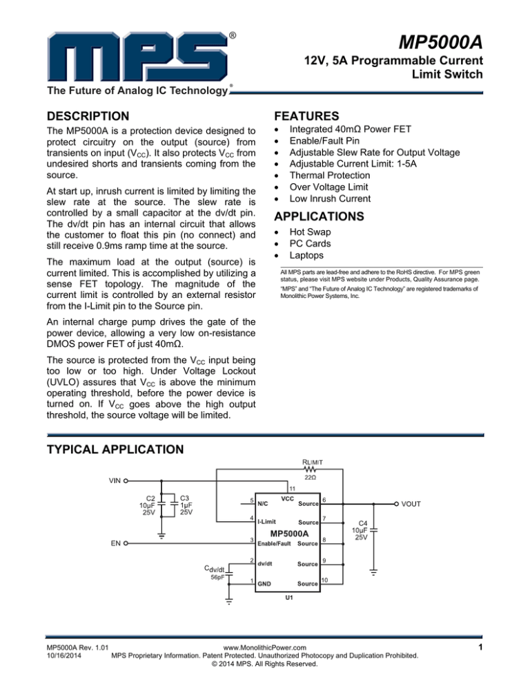
TYPICAL APPLICATION
MP5000A Rev. 1.01
www.MonolithicPower.com
10/16/2014
MPS Proprietary Information. Patent Protected. Unauthorized Photocopy and Duplication Prohibited.
© 2014 MPS. All Rights Reserved.
1
MP5000A – 12V, 1A-5A PROGRAMMABLE CURRENT LIMIT SWITCH
ORDERING INFORMATION
Part Number*
Package
Top Marking
MP5000ADQ
QFN-10 (3mmX3mm)
See Blow
* For Tape & Reel, add suffix –Z (e.g. MP5000ADQ–Z);
For RoHS Compliant Packaging, add suffix –LF (e.g. MP5000ADQ–LF–Z)
TOP MARKING
AHQY
LLL
AHQ: product code of MP5000ADQ;
Y: year code;
LLL: lot number;
PACKAGE REFERENCE
TOP VIEW
GND
1
DV/DT
2
ENABLE/FAULT
3
I-LIMIT
4
N/C
5
EXPOSED
PAD
VCC
10
SOURCE
9
SOURCE
8
SOURCE
7
SOURCE
6
SOURCE
QFN-10 (3mmX3mm)
MP5000A Rev. 1.01
www.MonolithicPower.com
10/16/2014
MPS Proprietary Information. Patent Protected. Unauthorized Photocopy and Duplication Prohibited.
© 2014 MPS. All Rights Reserved.
2
MP5000A – 12V, 1A-5A PROGRAMMABLE CURRENT LIMIT SWITCH
•
ABSOLUTE MAXIMUM RATINGS
(1)
VCC, SOURCE, I-LIMIT ...................-0.3V to 22V
dv/dt, ENABLE/FAULT .....................-0.3V to 6V
Storage Temperature............... -65°C to +155°C
(2)
Continuous Power Dissipation (TA = +25°C)
............................................................. 2.5W
Operating Junction Temperature. -40°C to 150°C
Input Voltage Transient (100mS) ......... VIN=25V
Recommended Operating Conditions
(3)
Input Voltage Operating Range…….10V to 18V
Continuous Current
0.5 in2 pad .................................................. 4.2A
For Minimum Copper, TA=80°C .................. 2.3A
Operating Junction Temp. (TJ). -40°C to +125°C
Thermal Resistance
(4)
θJA
θJC
QFN-10 (3mmX3mm) .............50 ...... 12 ... °C/W
Notes:
1) Exceeding these ratings may damage the device.
2) The maximum allowable power dissipation is a function of the
maximum junction temperature TJ(MAX), the junction-toambient thermal resistance θJA, and the ambient temperature
TA. The maximum allowable continuous power dissipation at
any ambient temperature is calculated by PD(MAX)=(TJ(MAX)TA)/ θJA. Exceeding the maximum allowable power dissipation
will cause excessive die temperature, and the regulator will go
into thermal shutdown. Internal thermal shutdown circuitry
protects the device from permanent damage.
3) The device is not guaranteed to function outside of its
operating conditions.
4) Measured on JESD51-7, 4-layer PCB.
MP5000A Rev. 1.01
www.MonolithicPower.com
10/16/2014
MPS Proprietary Information. Patent Protected. Unauthorized Photocopy and Duplication Prohibited.
© 2014 MPS. All Rights Reserved.
3
MP5000A – 12V, 1A-5A PROGRAMMABLE CURRENT LIMIT SWITCH
ELECTRICAL CHARACTERISTICS
VCC = 12V, RLIMIT=22Ω, Capacitive Load = 100μF, TA=25°C, unless otherwise noted.
Parameters
Power FET
Symbol
Delay Time (5)
tDLY
ON Resistance
RDSon
Off State Output Voltage
VOFF
Thermal Latch
Shutdown Temperature(6)
Under/Over Voltage Protection
TSD
Output Clamping Voltage
VCLAMP
Under Voltage Lockout
VUVLO
Under Voltage Lockout (UVLO)
Hysteresis
Current Limit
Hold Current (7)
Trip Current (7)
dv/dt Circuit
Min
Enabling
of
chip
to
ID=100mA with a 1A resistive
load
TJ=25°C
TJ=85°C (6)
VCC=18Vdc, VENABLE=0Vdc,
RL= 500Ω
ILIM-SS
ILIM-OL
Tr
Enable/Fault
Low Level Input Voltage
VIL
Intermediate Level Input Voltage
VI (INT)
High Level Input Voltage
High State Maximum Voltage
Low Level Input Current (Sink)
VIH
VI (MAX)
IIL
Maximum Fanout for Fault Signal
Typ
Max
Units
0.4
40
52
ms
55
mΩ
120
mV
175
Overvoltage Protection
VCC=17V
Turn on,
Voltage going high
°C
13.8
15
16.2
V
7.7
8.5
9.3
V
VHYST
Rise Time
Maximum Voltage on Enable/Fault
Pin (8)
Total Device
Condition
0.80
RLIM=22Ω
RLIM=22Ω
Float dv/dt pin, Output rises
from 10% to 90%
Output Disabled
Thermal
Fault,
Disabled
Output Enabled
Output
VENABLE=0V
Total number of chips that
can be connected for
simultaneous shutdown
2.3
3.6
4.7
4.9
A
A
0.4
0.9
2.1
ms
0.5
V
1.95
V
-50
V
V
μA
3
Units
VCC
V
0.82
1.4
2.5
5
-28
VMAX
Bias Current
IBIAS
Device Operational
Thermal Shutdown
Minimum Operating Voltage for
UVLO
VMIN
Enable<0.5V
V
1
0.4
1.2
5
mA
V
Notes:
5) Related to Rise Time. See description in Fault and Enable Pin Section.
6) Guaranteed by design.
7) Guaranteed by characterization Test.
8) Maximum Input Voltage on Enable pin to be ≤ 6.0V if Vcc ≥ 6.0V, Maximum Input Voltage on Enable pin to be Vcc if Vcc ≤ 6.0V.
MP5000A Rev. 1.01
www.MonolithicPower.com
10/16/2014
MPS Proprietary Information. Patent Protected. Unauthorized Photocopy and Duplication Prohibited.
© 2014 MPS. All Rights Reserved.
4
MP5000A – 12V, 1A-5A PROGRAMMABLE CURRENT LIMIT SWITCH
PIN FUNCTIONS
Pin #
Name
Description
1
GND
2
dv/dt
3
Enable/Fault
4
I-Limit
Negative Input Voltage to the Device. This is used as the internal reference for the IC.
The internal dv/dt circuit controls the slew rate of the output voltage at turn on. It has an
internal capacitor that allows it to ramp up over the period of 0.9ms. An external
capacitor can be added to this pin to increase the ramp time. If an additional time delay
is not required, this pin should be left open.
The Enable/Fault pin is a tri-state, bi-directional interface. It can be used to enable the
output of the device by floating the pin, or disable the chip by pulling it to ground (using
an open drain or open collector device). If a thermal fault occurs, the voltage on this pin
will go to an intermediate state to signal a monitoring circuit that the device is in thermal
shutdown. See text: “ENABLE/FAULT PIN”.
A resistor between this pin and the Source pin sets the overload and short circuit
current limit levels.
DO NOT CONNECT. Pin must be left floating.
This pin is the source of the internal power FET and the output terminal of the IC.
5
6-10
11
N/C
SOURCE
VCC
Positive input voltage to the device (exposed pad).
(Exposed Pad)
MP5000A Rev. 1.01
www.MonolithicPower.com
10/16/2014
MPS Proprietary Information. Patent Protected. Unauthorized Photocopy and Duplication Prohibited.
© 2014 MPS. All Rights Reserved.
5
MP5000A – 12V, 1A-5A PROGRAMMABLE CURRENT LIMIT SWITCH
TYPICAL PERFORMANCE CHARACTERISTICS
VIN = 12V, VEN=3.3V, RLIMIT=22Ω, COUT=10uF, Cdv/dt=1nF, TA=25°C, unless otherwise noted.
MP5000A Rev. 1.01
www.MonolithicPower.com
10/16/2014
MPS Proprietary Information. Patent Protected. Unauthorized Photocopy and Duplication Prohibited.
© 2014 MPS. All Rights Reserved.
6
MP5000A – 12V, 1A-5A PROGRAMMABLE CURRENT LIMIT SWITCH
TYPICAL PERFORMANCE CHARACTERISTICS (continued)
VIN = 12V, VEN=3.3V, RLIMIT=22Ω, COUT=10uF, Cdv/dt=1nF, TA=25°C, unless otherwise noted.
MP5000A Rev. 1.01
www.MonolithicPower.com
10/16/2014
MPS Proprietary Information. Patent Protected. Unauthorized Photocopy and Duplication Prohibited.
© 2014 MPS. All Rights Reserved.
7
MP5000A – 12V, 1A-5A PROGRAMMABLE CURRENT LIMIT SWITCH
TYPICAL PERFORMANCE CHARACTERISTICS (continued)
VIN = 12V, VEN=3.3V, RLIMIT=22Ω, COUT=10uF, Cdv/dt=1nF, TA=25°C, unless otherwise noted.
MP5000A Rev. 1.01
www.MonolithicPower.com
10/16/2014
MPS Proprietary Information. Patent Protected. Unauthorized Photocopy and Duplication Prohibited.
© 2014 MPS. All Rights Reserved.
8
MP5000A – 12V, 1A-5A PROGRAMMABLE CURRENT LIMIT SWITCH
BLOCK DIAGRAM
VCC
5V
Charge
Pump
U1
28 A
Enable/
Fault
2.5V
2V Hys
U3
D1
R1
28k
M1
U2
RESET
Source
Latch
Control Logic
SET
Current Limit
Thermal
Shutdown
VCC UVLO
Voltage
Clamp
dv /dt
Control
I-Limit
dv/dt
GND
Figure 1—Function Block Diagram
MP5000A Rev. 1.01
www.MonolithicPower.com
10/16/2014
MPS Proprietary Information. Patent Protected. Unauthorized Photocopy and Duplication Prohibited.
© 2014 MPS. All Rights Reserved.
9
MP5000A – 12V, 1A-5A PROGRAMMABLE CURRENT LIMIT SWITCH
OPERATION
The MP5000A is designed to limit the in-rush
current to the load. It offers an integrated solution
to monitor the input voltage, output voltage,
output current and die temperature.
Under Voltage Lock Out Operation
If the supply (input) is below the UVLO threshold,
the output is disabled, and the fault line is driven
low.
When the supply goes above the UVLO
threshold, the output is enabled and the fault line
is released. When the fault line is released it will
be pulled high by a 28uA current source. No
external pull up resistor is required. In addition,
the pull up voltage is limited to 5 volts.
Output Over Voltage Protection
If the input voltage is higher than the OVP
threshold, the output will be clamped at 15V
(typical).
Current Limit
When the part is active, if load reaches trip
current (minimum threshold current triggering
over current protection) or a short is present, the
part switches into to a constant-current (hold
current) mode. Part will be shutdown only if the
over current condition stays long enough to
trigger thermal protection.
However, when the part is powered up by VCC or
EN, the load current should be smaller than hold
current. Otherwise, the part can’t be fully turned
on.
In a typical application using a current limit
resistor of 22Ω, the trip current will be 4.7A and
the hold current will be 3.6A. If the device is in its
normal operating state and passing 2.0A it will
need to dissipate only 160mw with the very low
on resistance of 40mΩ. For the package
dissipation of 50°C/Watt, the temperature rise will
only be + 8°C. Combined with a 25°C ambient,
this is only 33°C total package temperature.
During a short circuit condition, the device now
has 12V across it and the hold current clamps at
3.6A and therefore must dissipate 43W. At
50°C/watt, if uncontrolled, the temperature would
rise above the MP5000A thermal protection
(+175°C) and shutdown the device to cause the
temperature to drop below a hysteresis level.
Proper heat sink must be used if the device is
intended to supply the hold current and not
shutdown. Without a heat sink, hold current
should be maintained below 250mA at + 25°C
and below 150mA at +85°C to prevent the device
from activating the thermal shutdown feature.
Thermal protection
When thermal protection is triggered, the output
is disabled and the fault line is driven to the
middle level. The thermal fault condition is
latched, and the part will remain latch off state
until restart the power or reset the enable pin.
Enable / Fault Pin
The Enable/Fault Pin is a Bi-Directional three
levels I/O with a weak pull up current (28uA
typical). The three levels are low, mid and high. It
functions to enable/disable the part and to relay
Fault information.
Enable/Fault pin as an input:
1.
Low and mid disable the part.
2.
Low, in addition to disabling the part,
clears the fault flag.
3.
High enables the part (if the fault flag is
clear) after a delay time. The delay time
can be calculated by:
Tdelay = 80us +
1
t rise
3
Enable/Fault pin as an output:
1. The pull up current may (if not over ridden)
allow a “wired nor” pull up to enable the
part.
2.
An under voltage will cause a low on the
Enable/Fault pin, and will clear the fault
flag.
3.
A thermal fault will cause a mid level on
the Enable/Fault pin, and will set the fault
flag.
The Enable/Fault line must be above the mid
level for the output to be turned on.
The fault flag is an internal flip-flop that can be
set or reset under various conditions:
MP5000A Rev. 1.01
www.MonolithicPower.com
10/16/2014
MPS Proprietary Information. Patent Protected. Unauthorized Photocopy and Duplication Prohibited.
© 2014 MPS. All Rights Reserved.
10
MP5000A – 12V, 1A-5A PROGRAMMABLE CURRENT LIMIT SWITCH
1.
Thermal Shutdown: set fault flag
2.
Under Voltage: reset fault flag
3.
low voltage on Enable/Fault pin: reset
fault flag
4.
mid voltage on Enable/Fault pin: no effect
Under a fault, the Enable/Fault pin is driven to
the mid level.
There are 4 types of faults, and each fault has a
direct and indirect effect on the Enable/Fault pin
and the internal fault flag.
In a typical application there are one or more of
the MP5000A chips in a system. The
Enable/Fault lines will typically be connected
together.
Table 1—Fault Function Influence in Application
Fault description
Internal action
Effect on Fault Pin
Short/over current
Limit current
none
Under Voltage
Output is
turned off
Internally drives
Enable/Fault pin to
Logic low
Over Voltage
Limit output
voltage
None
Thermal
Shutdown
Shutdown part
The part is
latched off until
a UVLO or
externally driven
to ground.
Internally drives
Enable/Fault pin
to mid level
Effect on Flag
none
Flag is reset
None
Flag is set
Effect on secondary Part
none
Secondary part output is
disabled, and fault flag is
reset.
None
Secondary part output is
disabled.
MP5000A Rev. 1.01
www.MonolithicPower.com
10/16/2014
MPS Proprietary Information. Patent Protected. Unauthorized Photocopy and Duplication Prohibited.
© 2014 MPS. All Rights Reserved.
11
MP5000A – 12V, 1A-5A PROGRAMMABLE CURRENT LIMIT SWITCH
APPLICATION INFORMATION
Current Limit
The desired current limit is a function of the
external current limit resistor.
Table 2—Current Limit vs. Current Limit Resistor
(VCC=12V)
RLIMIT (Ω)
Trip
Current (A)
Hold
Current (A)
15.4
18.2
22
30
51
100
5.93
5.26
4.70
3.71
2.84
2.28
5.28
4.37
3.60
2.56
1.52
0.81
PCB LAYOUT
PCB layout is very important to achieve stable
operation. Please follow these guidelines and
take below figure for reference. Place Rlimit
close to I_limit pin, Cdv/dt close to dv/dt pin and
input cap close to VCC pin. Keep the N/C pin float.
Put vias in thermal pad and ensure enough
copper area near VCC and source to achieve
better thermal performance.
VIN
VOUT
C2
Rise Time
The rise time is a function of the capacitor (Cdvdt)
on the dv/dt pin.
C3
EN/ FAULT
50pF
500pF
1nF
0.9
2
12
23
10 SOURCE
dv/dt
2
9 SOURCE
EN/ FAULT
3
I_LIMIT
4
N/C
5
8 SOURCE
VIN
RLIMIT
7 SOURCE
6 SOURCE
C4
none
1
Cdv/dt
Table 3—Rise Time vs. Cdv/dt
Cdvdt
Rise Time
(TYPICAL) (ms)
GND
* Notes: Rise Time = KRT*(41pF+Cdv/dt), KRT =22E6
The “rise time” is measured by from 0% to 100%
of output voltage.
GND
Top Layer
U
Input
Output
100%
Enable
0%
Rise Time
t
Figure 2—Rise Time
VIN
Bottom Layer
Figure 3―PCB Layout
MP5000A Rev. 1.01
www.MonolithicPower.com
10/16/2014
MPS Proprietary Information. Patent Protected. Unauthorized Photocopy and Duplication Prohibited.
© 2014 MPS. All Rights Reserved.
12
MP5000A – 12V, 1A-5A PROGRAMMABLE CURRENT LIMIT SWITCH
Design Example
Below is a design example following the
application guidelines for the given specifications:
Table 4: Design Example
VIN
Trip Current
Hold Current
12V
4.7A
3.6A
Figure 4 shows the application schematic. The
Typical Performance Characteristics section
shows the circuit waveforms. For more device
applications, please refer to the related
Evaluation Board Datasheet.
TYPICAL APPLICATION CIRCUITS
Figure 4―Typical Application Schematic
MP5000A Rev. 1.01
www.MonolithicPower.com
10/16/2014
MPS Proprietary Information. Patent Protected. Unauthorized Photocopy and Duplication Prohibited.
© 2014 MPS. All Rights Reserved.
13
MP5000A – 12V, 1A-5A PROGRAMMABLE CURRENT LIMIT SWITCH
PACKAGE INFORMATION
QFN10 (3 x 3mm)
2.90
3.10
0.30
0.50
PIN 1 ID
MARKING
0.18
0.30
2.90
3.10
PIN 1 ID
INDEX AREA
1.45
1.75
PIN 1 ID
SEE DETAIL A
10
1
2.25
2.55
0.50
BSC
5
6
TOP VIEW
BOTTOM VIEW
PIN 1 ID OPTION A
R0.20 TYP.
PIN 1 ID OPTION B
R0.20 TYP.
0.80
1.00
0.20 REF
0.00
0.05
SIDE VIEW
DETAIL A
NOTE:
2.90
0.70
1) ALL DIMENSIONS ARE IN MILLIMETERS.
2) EXPOSED PADDLE SIZE DOES NOT INCLUDE MOLD FLASH.
3) LEAD COPLANARITY SHALL BE 0.10 MILLIMETER MAX.
4) DRAWING CONFORMS TO JEDEC MO-229, VARIATION VEED-5.
5) DRAWING IS NOT TO SCALE.
1.70
0.25
2.50
0.50
RECOMMENDED LAND PATTERN
NOTICE: The information in this document is subject to change without notice. Users should warrant and guarantee that third
party Intellectual Property rights are not infringed upon when integrating MPS products into any application. MPS will not
assume any legal responsibility for any said applications.
MP5000A Rev 1.01
www.MonolithicPower.com
10/16/2014
MPS Proprietary Information. Patent Protected. Unauthorized Photocopy and Duplication Prohibited.
© 2014 MPS. All Rights Reserved.
14

