CAEN
Tools for Discovery
DS2631
n
A1422
Low Noise Fast Rise Time Charge Sensitive Preamplifier
Data Sheet
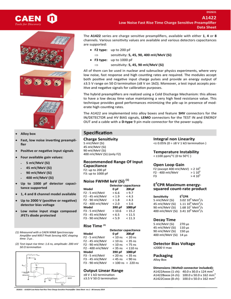
The A1422 series are charge sensitive preamplifiers, available with either 1, 4 or 8
channels. Various sensitivity values are available and various detectors capacitances
are supported:
F2 type:
F3 type:
up to 200 pF
sensitivity: 5, 45, 90, 400 mV/MeV (Si)
up to 1000 pF
sensitivity: 5, 45, 90 mV/MeV (Si)
All of them can be used in nuclear and subnuclear physics experiments, where very
low noise, fast response and high counting rates are required. The modules accept
both positive and negative input charge pulses and provide an energy output of
±3.5 V range on 50 Ω termination (±8 V on 1kΩ). Moreover, a test input accepts positive and negative signals for calibration purposes.
The hybrid preamplifiers are realized using a Cold Discharge Mechanism: this allows
to have a low decay time value maintaining a very high feed resistance value. This
technique provides good performances minimizing the pile-up in presence of moderate high counting rates.
The A1422 are implemented into alloy boxes and feature SHV connectors for the
IN/DETECTOR and HV BIAS signals, LEMO connectors for the TEST IN and ENERGY
OUT and a cable with a D-type 9 pin male connector for the power supply.
Alloy box
Specification
Fast, low noise inverting preamplifier
Charge Sensitivity
Integral non Linearity
5 mV/MeV (Si)
45 mV/MeV (Si)
90 mV/MeV (Si)
400 mV/MeV (Si) (only F2)
<± 0.05% (0 ÷ ±8 V 1 kΩ termination )
Positive or negative input signals
Four available gain values:
Recommended Range Of Input
Capacitance
5 mV/MeV (Si)
45 mV/MeV (Si)
90 mV/MeV (Si)
400 mV/MeV (Si)
F2: up to 200 pF
F3: up to 1000 pF
Up to 1000 pF detector capacitance supported
1, 4 and 8 channel model available
Up to 2000 V (positive or negative)
detector bias voltage
Low noise input stage composed
JFETs diode protected
Noise FWHM keV (Si) (1)
Model
F2 - 5 mV/MeV
F2 - 45 mV/MeV
F2 - 90 mV/MeV
F2 - 400 mV/MeV
Model
F3 - 5 mV/MeV
F3 - 45 mV/MeV
F3 - 90 mV/MeV
Rise Time
(1) Measured with a CAEN N968 Spectroscopy
Amplifier and N957 Peak Sensing ADC shaping
time: 3 µs .
(2) Test input rise time: 1.6 ns, amplitude: 200 mV
50 Ω termination
Vbias
Rbias
RF
CF
Detector capacitance
0 pF
200 pF
< 6.6
< 9.7
< 1.9
< 4.3
< 1.8
< 4.3
< 2.0
< 3.6
390 pF 1000 pF
< 10.6 < 15.2
< 6.5
< 11.5
< 5.9
< 11.3
(2)
Model
F2 - 5 mV/MeV
F2 - 45 mV/MeV
F2 - 90 mV/MeV
F2 - 400 mV/MeV
Model
F3 - 5 mV/MeV
F3 - 45 mV/MeV
F3 - 90 mV/MeV
Detector capacitance
0 pF
200 pF
< 10 ns < 20 ns
< 10 ns < 35 ns
< 10 ns < 75 ns
< 35 ns < 110 ns
390 pF 1000 pF
< 20 ns < 35 ns
< 45 ns < 90 ns
< 100 ns < 220 ns
Output Linear Range
From
detector
50 Ω
R2
±8 V 1 kΩ termination
±3.5 V 50 Ω termination
R1
DS2631 - A1422H Low Noise Fast Rise Time Charge Sensitive Preamplifier Data Sheet rev.1 - 08 January 2014
Temperature Instability
< ±100 ppm/°C (0 to 50°C )
Open Loop Gain
F2 (except 400 mV/MeV) > 2 105
F2 - 400 mV/MeV
> 1 106
F3
> 4 105
E2CPR Maximum energysquared count-rate product
Sensitivity
5 mV/MeV (Si)
45 mV/MeV (Si)
90 mV/MeV (Si)
400 mV/MeV (Si)
E2CPR
3.02 108 MeV2/s
1.11 108 MeV2/s
1.68 107 MeV2/s
3.41 106 MeV2/s
Decay Time
5 mV/MeV (Si)
45 mV/MeV (Si)
90 mV/MeV (Si)
400 mV/MeV (Si)
270 µs
110 µs
150 µs
14 µs
Detector Bias Voltage
±2000 V max
Packaging
Alloy Box
Dimensions (WxHxD connector included):
A1422Axxxx (1 ch): 40.0 x 30.0 x 124 mm3
A1422Bxxxx (4 ch): 100.0 x 50.0 x 162 mm3
A1422Cxxxx (8 ch): 100.0 x 50.0 x 162 mm3
CAEN
DS2631
n
Tools for Discovery
A1422
Low Noise Fast Rise Time Charge Sensitive Preamplifier
Data Sheet
Fig. 1 : Typical Rise Time vs input Capacitance (test input rise time = 1.6 ns, amplitude: 200 mV, 50 Ω termination)
Noise (F3 type)
20,0
18,0
16,0
14,0
12,0
10,0
8,0
6,0
4,0
2,0
0,0
F2-5
F2-45
F2-90
F2-400
1
10
100
Noise FWHM (keV)
Noise FWHM (keV)
Noise (F2 type)
18
16
14
12
10
8
6
4
2
-
1000
F3-5
F3-45
F3-90
1
Input Capacitance (pF)
10
100
1000
Input Capacitance (pF)
Fig. 2: Maximum Noise vs input Capacitance
Inputs
Input/Detector
Accepts positive and negative input charge
pulses from semiconductor detectors and
supplies the HV bias to the detector itself;
SHV connector.
High Voltage Bias
Up to 2000 V (positive or negative) for the
detector bias. 100 MΩ resistance in series
(other on request); SHV connector (BNC on
request).
Test
Positive or negative input for the energy
calibration via Ctest = 1 pF or 10 pF (on 5
mV/MeV versions); LEMO-00 connector.
Outputs
Power Requirements
Models
A1422AxxxF2 (1 ch):
A1422BxxxF2 (4 ch):
A1422CxxxF2 (8 ch):
+12 V
14 mA
55 mA
105 mA
-12 V
6 mA
25 mA
50 mA
A1422AxxxF3 (1 ch):
A1422BxxxF3 (4 ch):
A1422CxxxF3 (8 ch):
24 mA 6 mA
80 mA 25 mA
160 mA 50 mA
The power supply can be provided by CAEN
Spectroscopy Amplifier N968 (via a D-type
female connector on the rear-panel) or
DT5423 Desktop Linear Power Supply.
Output/Energy
± 8V max. (open circuit), 50 Ω back termination. The output voltage is proportional
to the amount of input charge.
Connector:
- A1422A (1 ch):
BNC
- A1422B/C (4/8 ch): LEMO-00
The typical rise time is
Detector capacitance = 0 pF
< 10 ns F2 - 5/45/90 mV/MeV
< 35 ns F2 - 400 mV/MeV
Detector capacitance = 390 pF
< 20 ns F3 - 5 mV/MeV
< 45 ns F3 - 45 mV/MeV
< 100 ns F3 - 90 mV/MeV
Power
Input Power through a 2.1 m cable with a Dtype 9 pin male connector.
Adjacent Channel Crosstalk (4/8 ch) = -40 dB
with reverse polarity
Fig. 3: Power Supply Connector pin out
Panel Layout
Fig. 4: A1422 series Front and Rear panel 8ch, 4ch, 1ch (dimension: mm)
Ordering Option
Detector
capacitance pF
Gain mV/
MeV
5
45
< 200
90
400
5
< 1000
45
90
CAEN
Tools for Discovery
n
No. of
Channels
Ordering code
Description
1
WA1422A005F2
A1422A005F2 - 1 Ch. Charge Preamplifier, 5mV/MeVgain, Cdet<200pF
4
WA1422B005F2
A1422B005F2 - 4 Ch. Charge Preamplifier, 5mV/MeVgain, Cdet<200pF
8
WA1422C005F2
A1422C005F2 - 8 Ch. Charge Preamplifier, 5mV/MeVgain, Cdet<200pF
1
WA1422A045F2
A1422A045F2 - 1 Ch. Charge Preamplifier, 45mV/MeVgain, Cdet<200pF
4
WA1422B045F2
A1422B045F2 - 4 Ch. Charge Preamplifier, 45mV/MeVgain, Cdet<200pF
8
WA1422C045F2
A1422C045F2 - 8 Ch. Charge Preamplifier, 45mV/MeVgain, Cdet<200pF
1
WA1422A090F2
A1422A090F2 - 1 Ch. Charge Preamplifier, 90mV/MeVgain, Cdet<200pF
4
WA1422B090F2
A1422B090F2 - 4 Ch. Charge Preamplifier, 90mV/MeVgain, Cdet<200pF
8
WA1422C090F2
A1422C090F2 - 8 Ch. Charge Preamplifier, 90mV/MeVgain, Cdet<200pF
1
WA1422A400F2
A1422A400F2 - 1 Ch. Charge Preamplifier, 400mV/MeVgain, cdet<200pF
4
WA1422B400F2
A1422B400F2 - 4 Ch. Charge Preamplifier, 400mV/MeVgain, Cdet<200pF
1
WA1422A005F3
A1422A005F3 - 1 Ch. Charge Preamplifier, 5mV/MeVgain, Cdet<1000pF
4
WA1422B005F3
A1422B005F3 - 4 Ch. Charge Preamplifier, 5mV/MeVgain, Cdet<1000pF
8
WA1422C005F3
A1422C005F3 - 8 Ch. Charge Preamplifier, 5mV/MeVgain, Cdet<1000pF
1
WA1422A045F3
A1422A045F3 - 1 Ch. Charge Preamplifier, 45mV/MeVgain, Cdet<1000pF
4
WA1422B045F3
A1422B045F3 - 4 Ch. Charge Preamplifier, 45mV/MeVgain, Cdet<1000pF
8
WA1422C045F3
A1422C045F3 - 8 Ch. Charge Preamplifier, 45mV/MeVgain, Cdet<1000pF
1
WA1422A090F3
A1422A090F3 - 1 Ch. Charge Preamplifier, 90mV/MeVgain, Cdet<1000pF
4
WA1422B090F3
A1422B090F3 - 4 Ch. Charge Preamplifier, 90mV/MeVgain, Cdet<1000pF
8
WA1422C090F3
A1422C090F3 - 8 Ch. Charge Preamplifier, 90mV/MeVgain, Cdet<1000pF
CAEN SpA
Via Vetraia 11
55049 – Viareggio Italy
Tel +39.0584.388.398
Fax +39.0584.388.959
info@caen.it www.caen.it
2014 Copyright © CAEN SpA. All rights reserved. Information in this publication supersedes all earlier versions. Specifications subject to change without notice.
www.caen.it
