The Differential Amplifier BJT Differential Pair
advertisement
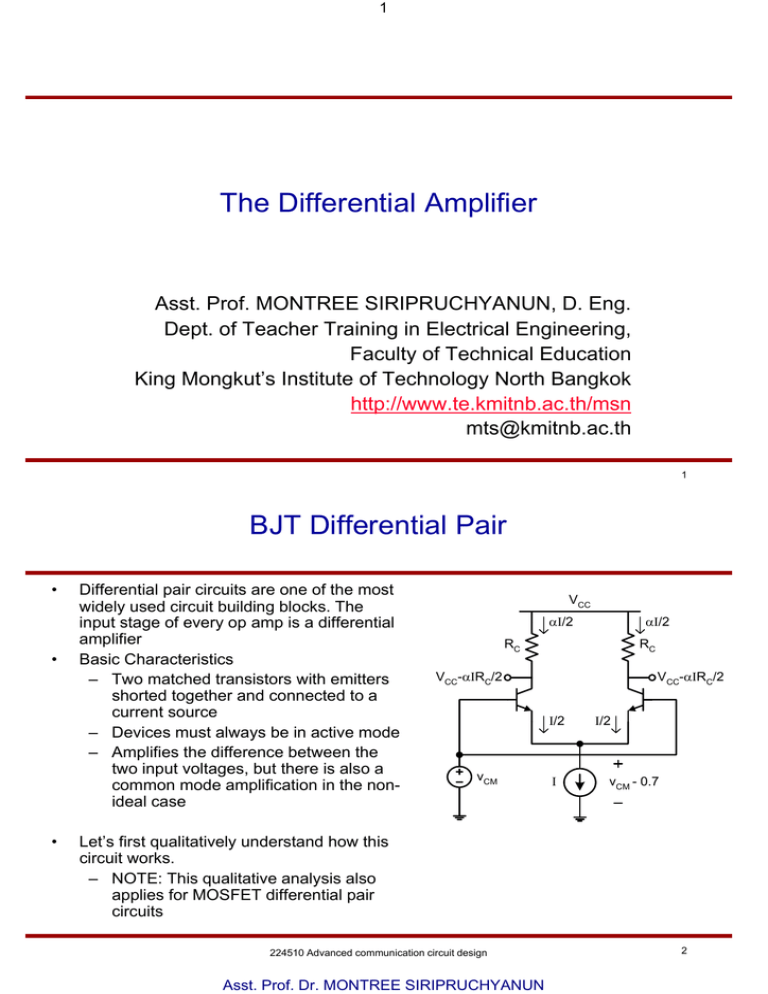
1 The Differential Amplifier Asst. Prof. MONTREE SIRIPRUCHYANUN, D. Eng. Dept. of Teacher Training in Electrical Engineering, Faculty of Technical Education King Mongkut’s Institute of Technology North Bangkok http://www.te.kmitnb.ac.th/msn mts@kmitnb.ac.th 1 BJT Differential Pair • • • Differential pair circuits are one of the most widely used circuit building blocks. The input stage of every op amp is a differential amplifier Basic Characteristics – Two matched transistors with emitters shorted together and connected to a current source – Devices must always be in active mode – Amplifies the difference between the two input voltages, but there is also a common mode amplification in the nonideal case VCC αI/2 αI/2 RC RC VCC-αIRC/2 VCC-αIRC/2 I/2 vCM I I/2 vCM - 0.7 Let’s first qualitatively understand how this circuit works. – NOTE: This qualitative analysis also applies for MOSFET differential pair circuits 224510 Advanced communication circuit design Asst. Prof. Dr. MONTREE SIRIPRUCHYANUN 2 2 Case 1 • • Assume the inputs are shorted together to a common voltage, vCM, called the common mode voltage – equal currents flow through Q1 and Q2 – emitter voltages equal and at vCM-0.7 in order for the devices to be in active mode – collector currents are equal and so collector voltages are also equal for equal load resistors – difference between collector voltages = 0 VCC αI/2 αI/2 RC VCC-αIRC/2 What happens when we vary vCM? – As long as devices are in active mode, equal currents flow through Q1 and Q2 – Note: current through Q1 and Q2 always add up to I, current through the current source – So, collector voltages do not change and difference is still zero…. – Differential pair circuits thus reject common mode signals RC Q1 Q2 I/2 vCM VCC-αIRC/2 I/2 vCM - 0.7 I 3 224510 Advanced communication circuit design Case 2 & 3 • Q2 base grounded and Q1 base at +1 V – All current flows through Q1 – No current flows through Q2 – Emitter voltage at 0.3V and Q2’s EBJ not FB – vC1 = VCC-αIRC – vC2 = VCC VCC αI 0 RC VCC-αIRC +1V RC Q1 I Q2 0 VCC 0 αI RC VCC -1V I RC Q1 Q2 0 I I -0.7V VCC-αIRC • 0.3V Q2 base grounded and Q1 base at -1 V – All current flows through Q2 – No current flows through Q1 – Emitter voltage at -0.7V and Q1’s EBJ not FB – vC2 = VCC-αIRC – vC1 = VCC 224510 Advanced communication circuit design Asst. Prof. Dr. MONTREE SIRIPRUCHYANUN 4 3 Case 4 • Apply a small signal vi – Causes a small positive ΔI to flow in Q1 – Requires small negative ΔI in Q2 • since IE1+IE2 = I • • – Can be used as a linear amplifier for small signals (ΔI is a function of vi) Differential pair responds to differences in the input voltage – Can entirely steer current from one side of the diff pair to the other with a relatively small voltage Let’s now take a quantitative look at the large-signal operation of the differential pair 224510 Advanced communication circuit design 5 BJT Diff Pair – Large-Signal Operation • First look at the emitter currents when the emitters are tied together • Some manipulations can lead to the following equations • and there is the constraint: • Given the exponential relationship, small differences in vB1,2 can cause all of the current to flow through one side 224510 Advanced communication circuit design Asst. Prof. Dr. MONTREE SIRIPRUCHYANUN 6 4 • • Notice vB1-vB2 ~= 4VT enough to switch all of current from one side to the other For small-signal analysis, we are interested in the region we can approximate to be linear – small-signal condition: vB1-vB2 < VT/2 224510 Advanced communication circuit design 7 BJT Diff Pair – Small-Signal Operation • Look at the small-signal operation: small differential signal vd is applied multiply top and bottom by – expand the exponential and keep the first two terms 224510 Advanced communication circuit design Asst. Prof. Dr. MONTREE SIRIPRUCHYANUN 8 5 Differential Voltage Gain • For small differential input signals, vd << 2VT, the collector currents are… • We can now find the differential gain to be… 9 224510 Advanced communication circuit design BJT Diff Pair – Differential Half Circuit • We can break apart the differential pair circuit into two half circuits – which then looks like two common emitter circuits driven by +vd/2 and –vd/2 Virtual Ground 224510 Advanced communication circuit design Asst. Prof. Dr. MONTREE SIRIPRUCHYANUN 10 6 Small-Signal Model of Diff Half Circuit • We can then analyze the small-signal operation with the half circuit, but must remember – parameters rπ,gm, and ro are biased at I / 2 – input signal to the differential half circuit is vd/2 vd/2 rπ vπ gmvπ vc1 ro RC – voltage gain of the differential amplifier (output taken differentially) is equal to the voltage gain of the half circuit 224510 Advanced communication circuit design 11 Common-Mode Gain • When we drive the differential pair with a common-mode signal, vCM, the incremental resistance of the bias current effects circuit operation and results in some gain (assumed to be 0 when R was infinite) 224510 Advanced communication circuit design Asst. Prof. Dr. MONTREE SIRIPRUCHYANUN 12 7 Common Mode Rejection Ratio • If the output is taken differentially, the output is zero since both sides move together. However, if taken single-endedly, the common-mode gain is finite • If we look at the differential gain on one side (single-ended), we get… • Then, the common rejection ratio (CMRR) will be – which is often expressed in dB 224510 Advanced communication circuit design 13 CM and Differential Gain Equation • Input signals to a differential pair usually consists of two components: common mode (vCM) and differential(vd) • Thus, the differential output signal will be in general… 224510 Advanced communication circuit design Asst. Prof. Dr. MONTREE SIRIPRUCHYANUN 14 8 MOS Diff Pair • The same basic analysis can be applied to a MOS differential pair – and the differential input voltage is – With some algebra… 224510 Advanced communication circuit design • 15 We get full switching of the current when… 224510 Advanced communication circuit design Asst. Prof. Dr. MONTREE SIRIPRUCHYANUN 16 9 Another Way to Analyze MOS Differential Pairs • • Let’s investigate another technique for analyzing the MOS differential pair Vout1 For the differential pair circuit on the left (driven by two independent signals), compute V in1 the output using superposition – Start with Vin1, set Vin2=0 and first solve for X w.r.t. Vin1 – Reduces to a degenerated common-source amp – neglecting channel-length modulation and bodyeffect, RS = 1/gm2 Vout1 – so… RD X RD Y RD Vout2 X Vout1 Vin2 RD Y Vin1 I RD X M1 Vin1 I RD RD Y Vout2 X Vout1 Vout2 Vin1 M2 RS RS 17 224510 Advanced communication circuit design Cont’d • • • Now, solve for Y w.r.t. Vin1 Replace circuit within box with a Thevenin equivalent – M1 is a source follower with VT=Vin1 – RT=1/gm1 The circuit reduces to a common-gate amplifier where… RD Vout1 RD X Y M1 Vout2 M2 Vin1 • So, overall (assuming gm1 = gm2) RD Y by symmetry Vout2 RT VT 224510 Advanced communication circuit design Asst. Prof. Dr. MONTREE SIRIPRUCHYANUN 18 10 Differential Pair with MOS loads • Can use load resistors or MOS devices as loads – Diode-connected nMOS loads = 1/gm load resistance • Load resistance looking into the source – Diode-connected pMOS loads = 1/gm load resistance • Load resistance looking into diode connected drain – pMOS current source loads = ro load resistance • Has higher gain than diode-connected loads – pMOS current mirror • Differential input and single-ended output 19 224510 Advanced communication circuit design Differential Pair with MOS Loads Vb Vout Vout Vin Vin I I • • Consider the above two MOS loads used in place of resistors Left: – a diode connected pMOS has an effective resistance of 1/gmP • Right: – pMOS devices in saturation have effective resistance of roP 224510 Advanced communication circuit design Asst. Prof. Dr. MONTREE SIRIPRUCHYANUN 20 11 Active-Loaded CMOS Differential Amplifier • • A commonly used amplifier topology in CMOS technologies Output is taken single-endedly for a differential input – with a vid/2 at the gate of M1, i1 flows M3 M4 i1 – – i1 is also mirrored through the M3-M4 current mirror a –vid/2 at the gate of M2 causes i2 to also flow through M2 vo i1 i2 M1 M2 vid • Given that ID= I / 2 (nominally) I • The voltage at the output then is given by… 224510 Advanced communication circuit design 21 Differential Amp with Linearized Gain • Use source generation to make the gain linear with respect to the differential input and independent of gm – Can build in two ways… 224510 Advanced communication circuit design Asst. Prof. Dr. MONTREE SIRIPRUCHYANUN 22 12 • Assuming a virtual ground at node X, we can draw the following small-signal half circuit. gmvπ vid vπ ro is RS RD vο vS – Assume ro is very large (simplifies the math) 224510 Advanced communication circuit design 23 Offsets in MOS Differential Pair • • There are 3 main sources of offset that affect the performance of MOS differential pair circuits – Mismatch in load resistors – Mismatch in W/L of differential pair devices – Mismatch in Vth of differential pair devices Let’s investigate each individually 224510 Advanced communication circuit design Asst. Prof. Dr. MONTREE SIRIPRUCHYANUN 24 13 Resistor Mismatch • • For the differential pair circuit shown, consider the case where – Load resistors are mismatched by ΔRD – All other device parameters are perfectly matched With both inputs grounded, I1 = I2= I/2, but VO is not zero due to differences in the voltages across the load resistors RD1 RD2 VO I1 I2 I – It is common to find the input-referred offset which is calculated as – since Ad = gmRD 224510 Advanced communication circuit design 25 W/L Mismatch • Now consider what happens when device sizes W/L are mismatched for the two differential pair MOS devices M1 and M2 • This mismatch causes mismatch in the currents that flow through M1 and M2 – This mismatch results in VO – So in the input referred offset is… 224510 Advanced communication circuit design Asst. Prof. Dr. MONTREE SIRIPRUCHYANUN 26 14 Vt Mismatch • Lastly, consider mismatches in the threshold voltage • Again, currents I1 and I2 will differ according to the following saturation current equation – For small ΔVt << 2(VGS-Vth) – Again, using VOS=VO/Ad (Ad = gmRD and VO =2ΔIRD) we get… 224510 Advanced communication circuit design 27 Mismatch Summary • The 3 sources of mismatch can be combined into one equation: • – arising from Vt, RD, and W/L mismatches Notice that offsets due to ΔRD and ΔW/L are functions of the overdrive voltage VGS – Vt 224510 Advanced communication circuit design Asst. Prof. Dr. MONTREE SIRIPRUCHYANUN 28
